


XAPP709 (v2.0) 2006 年 10 月 27 日 www.xilinx.com/cn 1
© 2004–2006 Xilinx, Inc. All rights reserved. All Xilinx trademarks, registered trademarks, patents, and further disclaimers are as listed at http://www.xilinx.com/legal.htm. All
other trademarks and registered trademarks are the property of their respective owners. All specifications are subject to change without notice.
NOTICE OF DISCLAIMER: Xilinx is providing this design, code, or information "as is." By providing the design, code, or information as one possible implementation of this
feature, application, or standard, Xilinx makes no representation that this implementation is free from any claims of infringement. You are responsible for obtaining any rights you
may require for your implementation. Xilinx expressly disclaims any warranty whatsoever with respect to the adequacy of the implementation, including but not limited to any
warranties or representations that this implementation is free from claims of infringement and any implied warranties of merchantability or fitness for a particular purpose.
提要 本应用指南描述了在 Virtex™-4 XC4VLX25 FF668 -10C 器件中实现的 DDR SDRAM 控制器。
该实现运用了直接时钟控制技术来实现数据采集,并采用自动校准电路来调整数据线上的延
迟。
DDR SDRAM 器件是低成本、高密度的存储资源,在很多存储器供应商处均可获得。本参考设
计使用 SDRAM 器件和 DIMM 开发而成。
DDR SDRAM
描述
DDR SDRAM 规范的详情可在电子工业联盟 (Electronic Industries Alliance, EIA) 成员 JEDEC
机构的网站上获得,网址为 http://www.jedec.org
/。DDR SDRAM 规范刊载在参考文件
JESD79E 下的 JEDEC 文档。
DDR SDRAM 器件是硅片存储器资源,现在最经常用于各种系统,包括从消费产品到视频系统
的各类应用。DDR SDRAM 器件的频率高达 200 MHz 或 DDR400。DRAM 可以使用器件或模
块的配置。
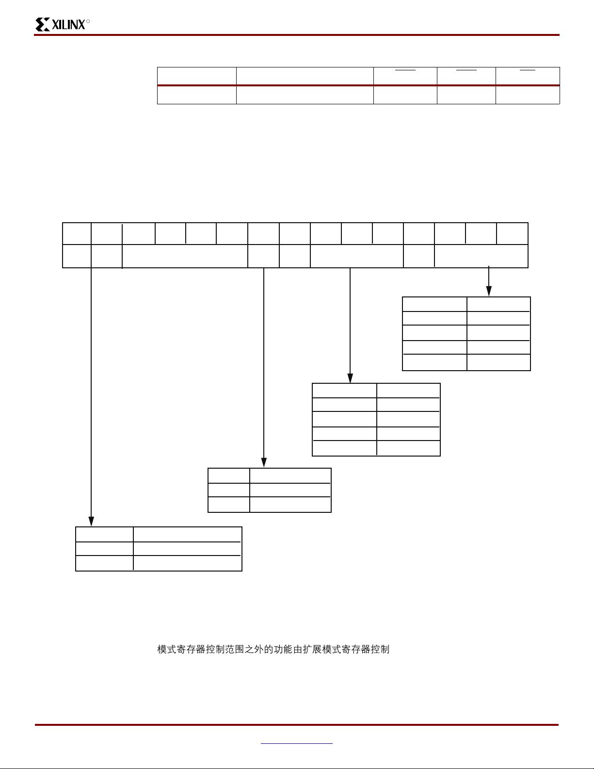
DDR 控制器命令
表1 所示为控制器发出的命令。这些命令通过使用下列控制信号传输到存储器:
• 行地址选择 (RAS
)
• 列地址选择 (CAS
)
• 写使能 (WE
)
• 时钟使能 (CKE) (器件配置后始终置为高)
• 芯片选择 (CS
) (器件运行期间始终置为低)
应用指南: Virtex-4 系列
XAPP709 (v2.0) 2006 年 10 月 27 日
使用 Virtex-4 FPGA 器件实现
DDR SDRAM 控制器
作者: Rich Chiu
R
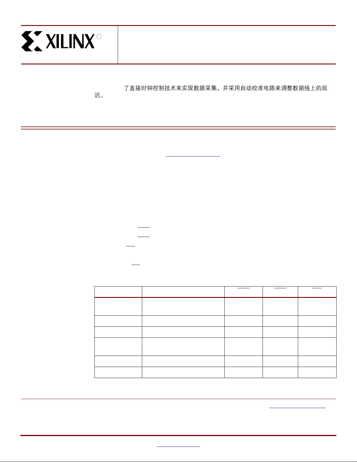
表 1:
DDR SDRAM 命令
信号编号 功能
RAS
CAS WE
1 加载模式寄存器 (Load Mode
Register)
LLL
2 自动刷新 (Auto Refresh) L L H
3 预充电 (Percharge)
(1)
LHL
4 选择组激活行 (Select Bank
Activate Row)
LHH
5 写命令 (Write Command) H L L
6 读命令 (Read Command) H L H


- 1
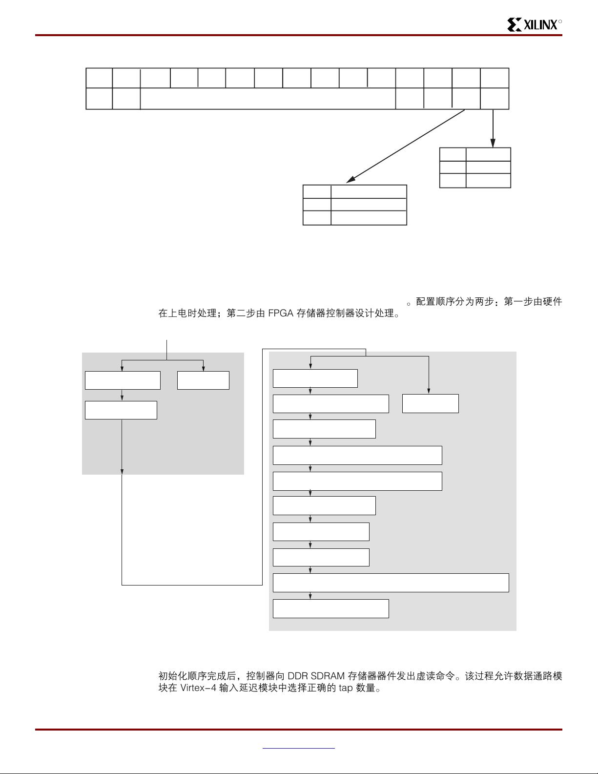
- 2
前往页