MC145170.pdf资料
需积分: 10 7 浏览量
2009-09-01
20:23:45
上传
评论
收藏 454KB PDF 举报

MC145170–1MOTOROLA
1
Advance Information
! !"
CMOS
The new MC145170–1 is pin–for–pin compatible with the MC145170. A
comparison of the two parts is shown in the table below. The MC145170–1 is
recommended for new designs.
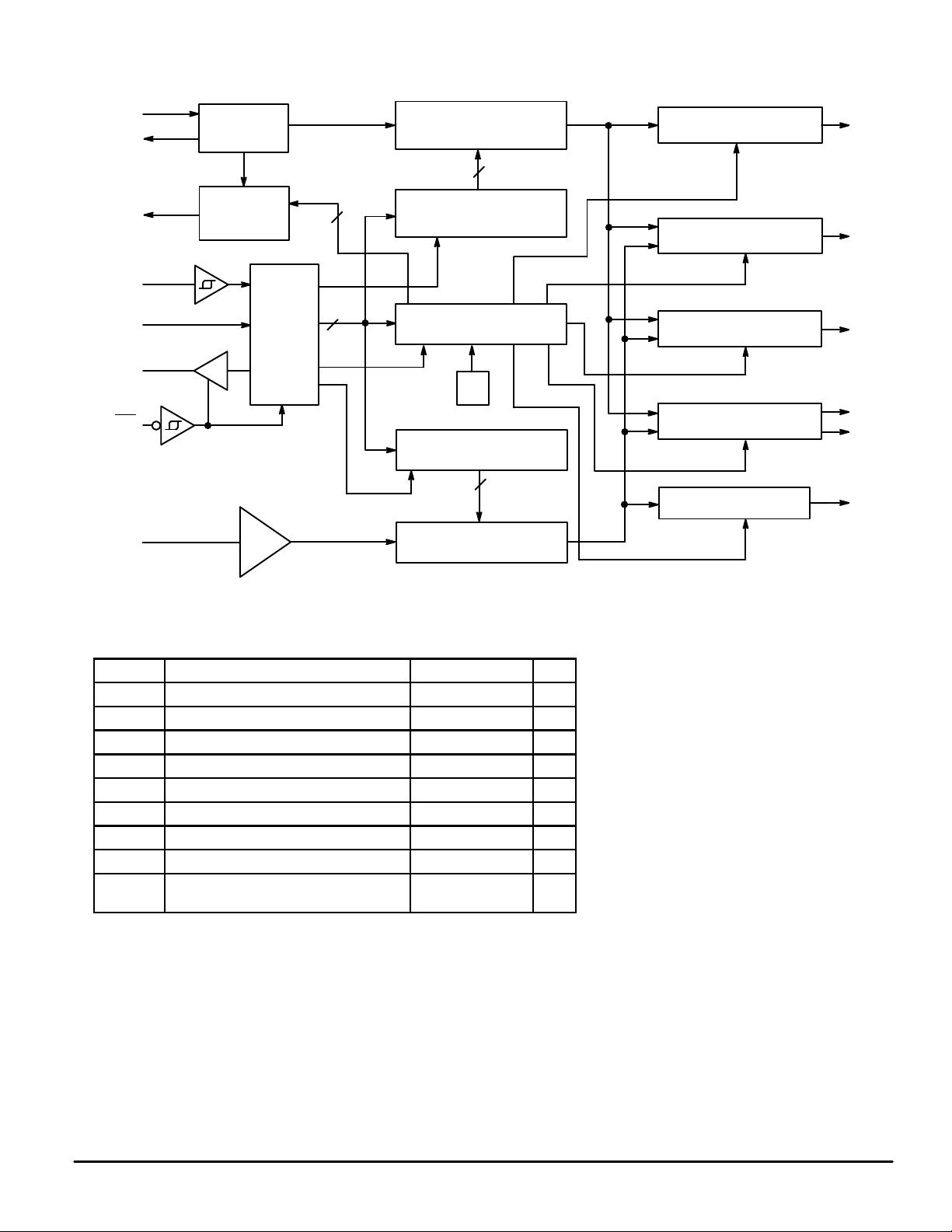
The MC145170–1 is a single–chip synthesizer capable of direct usage in the
MF, HF, and VHF bands. A special architecture makes this PLL the easiest to
program in the industry. Either a bit– or byte–oriented format may be used. Due
to the patented BitGrabber registers, no address/steering bits are required for
random access
of the three registers. Thus, tuning can be accomplished via a
2–byte serial transfer to the 16–bit N register.
The device features fully programmable R and N counters, an amplifier at the
f
in
pin, on–chip support of an external crystal, a programmable reference
output, and both single– and double–ended phase detectors with linear transfer
functions (no dead zones). A configuration (C) register allows the part to be
configured to meet various applications. A patented feature allows the C
register to shut off unused outputs, thereby minimizing noise and interference.
In order to reduce lock times and prevent erroneous data from being loaded
into the counters, a patented jam–load feature is included. Whenever a new
divide ratio is loaded into the N register, both the N and R counters are
jam–loaded with their respective values and begin counting down together. The
phase detectors are also initialized during the jam load.
• Operating Voltage Range: 2.5 to 5.5 V
• Maximum Operating Frequency:
185 MHz @ V
in
= 500 mV p–p, 4.5 V Minimum Supply
100 MHz @ V
in
= 500 mV p–p, 3.0 V Minimum Supply
• Operating Supply Current: 0.6 mA @ 3 V, 30 MHz
1.5 mA @ 3 V, 100 MHz
3.0 mA @ 5 V, 50 MHz
5.8 mA @ 5 V, 185 MHz
• Operating Temperature Range: – 40 to 85°C
• R Counter Division Range: 1 and 5 to 32,767
• N Counter Division Range: 40 to 65,535
• Direct Interface to Motorola SPI and National MICROWIRE Serial Data
Ports
• Chip Complexity: 4800 FETs or 1200 Equivalent Gates
• See Application Note AN1207/D
COMPARISION OF THE PLL FREQUENCY SYNTHESIZERS
Parameter MC145170–1 MC145170
Technology 1.2 µm CMOS 1.5 µm CMOS
Maximum Frequency with 5 V ± 10% Supply, f
in
185 MHz 160 MHz
Maximum Frequency with 5 V ± 10% Supply, OSC
in
25 MHz 20 MHz
Maximum Supply Voltage 5.5 V 6.0 V
Maximum Input Capacitance, f
in
7 pF 5 pF
This document contains information on a new product. Specifications and information herein are subject to change without notice.
BitGrabber is a trademark of Motorola Inc. MICROWIRE is a trademark of National Semiconductor Corp.
Order this document
by MC145170–1/D
SEMICONDUCTOR TECHNICAL DATA
f
R
LD
V
SS
9
10
11
12
φ
V
V
DD
PD
out
8
7
6
5
4
3
2
1
D
out
CLK
ENB
f
in
REF
out
OSC
out
OSC
in
14
15
16
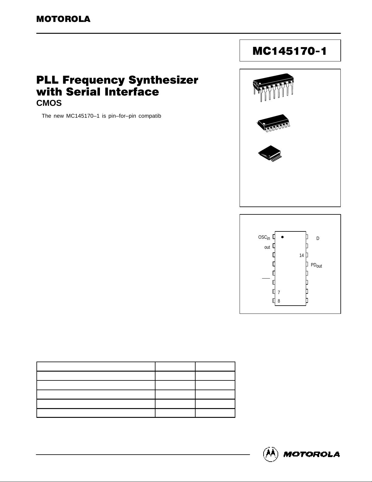
PIN ASSIGNMENT
D
in
f
V
P SUFFIX
PLASTIC DIP
CASE 648
D SUFFIX
SOG PACKAGE
CASE 751B
ORDERING INFORMATION
MC145170P1 Plastic DIP
MC145170D1 SOG Package
MC145170DT1 TSSOP
φ
R
16
1
13
DT SUFFIX
TSSOP
CASE 948C
16
1
16
1
Motorola, Inc. 1996
REV 1
3/96

剩余26页未读,继续阅读


评论0