没有合适的资源?快使用搜索试试~ 我知道了~
资源详情
资源评论
资源推荐
MAX 10 FPGA Device Datasheet
2015.01.23
M10-DATASHEET
Subscribe
Send Feedback
This datasheet describes the electrical characteristics, switching characteristics, configuration specifications, and timing for MAX
®
10 devices.
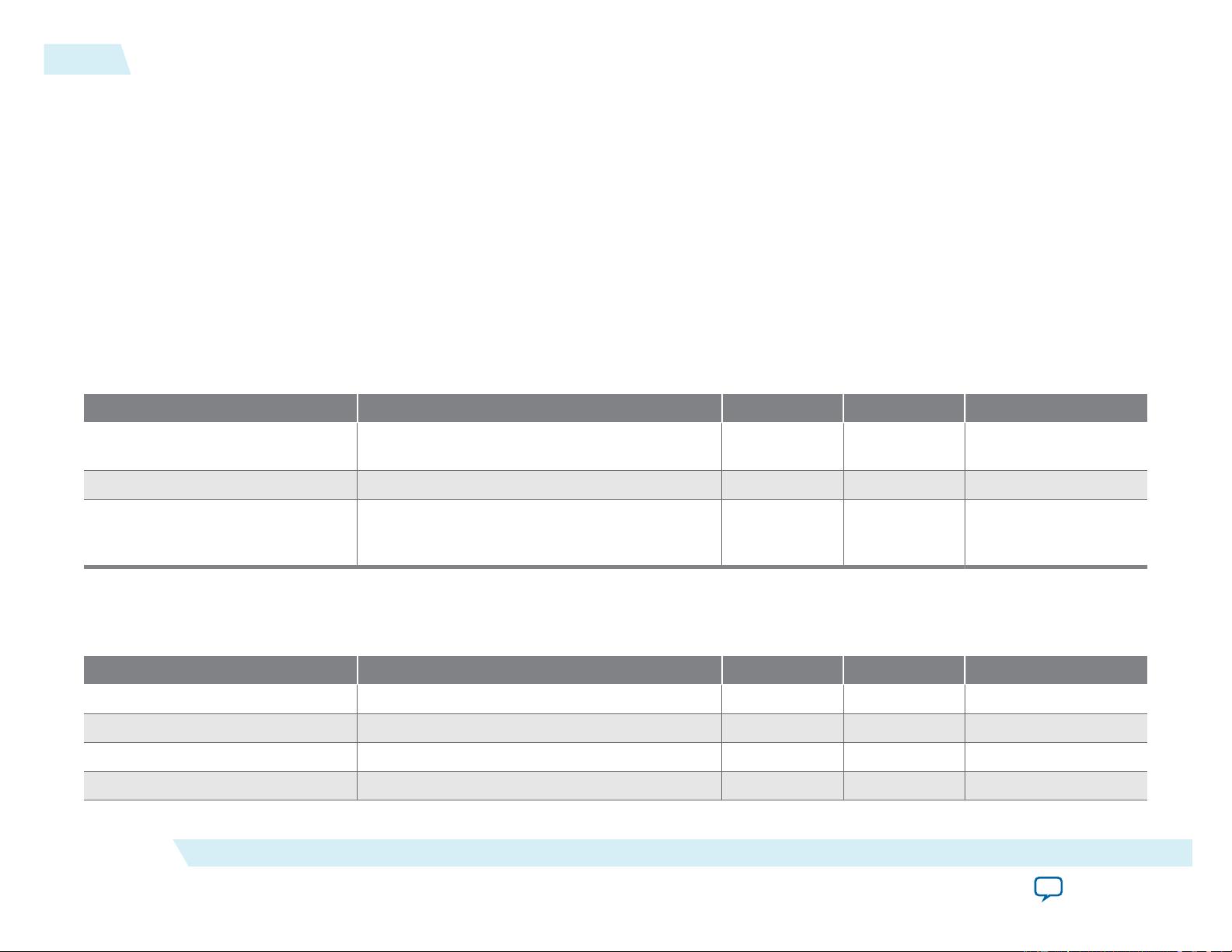
Table 1: MAX 10 Device Grades and Speed Grades Supported
Device Grade Speed Grade Supported
Commercial
• –C7
• –C8 (slowest)
Industrial
• –I6 (fastest)
• –I7
Automotive –A7
Note: The –I6 speed grade MAX 10 FPGA device option is not available by default in the Quartus
®
II software. Contact your local Altera sales
representatives for support.
Related Information
MAX 10 FPGA Device Overview
Provides more information about the densities and packages of devices in the MAX 10.
Electrical Characteristics
The following sections describe the operating conditions and power consumption of MAX 10 devices.
©
2015 Altera Corporation. All rights reserved. ALTERA, ARRIA, CYCLONE, ENPIRION, MAX, MEGACORE, NIOS, QUARTUS and STRATIX words and logos are trademarks of Altera Corporation and registered in the U.S. Patent
and Trademark Office and in other countries. All other words and logos identified as trademarks or service marks are the property of their respective holders as described at www.altera.com/common/legal.html. Altera
warrants performance of its semiconductor products to current specifications in accordance with Altera's standard warranty, but reserves the right to make changes to any products and services at any time without
notice. Altera assumes no responsibility or liability arising out of the application or use of any information, product, or service described herein except as expressly agreed to in writing by Altera. Altera customers are
advised to obtain the latest version of device specifications before relying on any published information and before placing orders for products or services.
ISO
9001:2008
Registered
www.altera.com
101 Innovation Drive, San Jose, CA 95134
Operating Conditions
MAX 10 devices are rated according to a set of defined parameters. To maintain the highest possible performance and reliability of the MAX 10
devices, you must consider the operating requirements described in this section.
Absolute Maximum Ratings
This section defines the maximum operating conditions for MAX 10 devices. The values are based on experiments conducted with the devices and
theoretical modeling of breakdown and damage mechanisms. The functional operation of the device is not implied for these conditions.
Caution: Conditions outside the range listed in the absolute maximum ratings tables may cause permanent damage to the device. Additionally,
device operation at the absolute maximum ratings for extended periods of time may have adverse effects on the device.
Single Supply Devices Absolute Maximum Ratings
Table 2: Absolute Maximum Ratings for MAX 10 Single Supply Devices—Preliminary
Symbol Parameter Min Max Unit
V
CC_ONE
Supply voltage for core and periphery through on-
die voltage regulator
–0.5 3.9 V
V
CCIO
Supply voltage for input and output buffers –0.5 3.9 V
V
CCA
Supply voltage for phase-locked loop (PLL)
regulator and analog-to-digital converter (ADC)
block (analog)
–0.5 3.9 V
Dual Supply Devices Absolute Maximum Ratings
Table 3: Absolute Maximum Ratings for MAX 10 Dual Supply Devices—Preliminary
Symbol Parameter Min Max Unit
V
CC
Supply voltage for core and periphery –0.5 1.63 V
V
CCIO
Supply voltage for input and output buffers –0.5 3.9 V
V
CCA
Supply voltage for PLL regulator (analog) –0.5 3.41 V
V
CCD_PLL
Supply voltage for PLL regulator (digital) –0.5 1.63 V
2
Operating Conditions
M10-DATASHEET
2015.01.23
Altera Corporation
MAX 10 FPGA Device Datasheet
Send Feedback
Symbol Parameter Min Max Unit
V
CCA_ADC
Supply voltage for ADC analog block –0.5 3.41 V
V
CCINT
Supply voltage for ADC digital block –0.5 1.63 V
Absolute Maximum Ratings
Table 4: Absolute Maximum Ratings for MAX 10 Devices—Preliminary
Symbol Parameter Min Max Unit
V
I
DC input voltage –0.5 4.12 V
I
OUT
DC output current per pin –25 25 mA
T
STG
Storage temperature –65 150 °C
T
J
Operating junction temperature –40 125 °C
Maximum Allowed Overshoot During Transitions over a 11.4-Year Time Frame
Table 5: Maximum Allowed Overshoot During Transitions over a 11.4-Year Time Frame for MAX 10 Devices
Condition (V) Overshoot Duration as % of High Time Unit
4.12 100.0 %
4.17 11.7 %
4.22 7.1 %
4.27 4.3 %
4.32 2.6 %
4.37 1.6 %
4.42 1.0 %
4.47 0.6 %
4.52 0.3 %
M10-DATASHEET
2015.01.23
Absolute Maximum Ratings
3
MAX 10 FPGA Device Datasheet
Altera Corporation
Send Feedback
Condition (V) Overshoot Duration as % of High Time Unit
4.57 0.2 %
Recommended Operating Conditions
This section lists the functional operation limits for the AC and DC parameters for MAX 10 devices. The tables list the steady-state voltage values
expected from MAX 10 devices. Power supply ramps must all be strictly monotonic, without plateaus.
Single Supply Devices Power Supplies Recommended Operating Conditions
Table 6: Power Supplies Recommended Operating Conditions for MAX 10 Single Supply Devices—Preliminary
Symbol Parameter Condition Min Typ Max Unit
V
CC_ONE
(1)
Supply voltage for core and periphery
through on-die voltage regulator
— 2.85/3.135 3.0/3.3 3.15/3.465 V
V
CCIO
(2)
Supply voltage for input and output
buffers
3.3 V 3.135 3.3 3.465 V
3.0 V 2.85 3 3.15 V
2.5 V 2.375 2.5 2.625 V
1.8 V 1.71 1.8 1.89 V
1.5 V 1.425 1.5 1.575 V
1.35 V 1.2825 1.35 1.4175 V
1.2 V 1.14 1.2 1.26 V
V
CCA
(1)
Supply voltage for PLL regulator and
ADC block (analog)
— 2.85/3.135 3.0/3.3 3.15/3.465 V
(1)
V
CCA
must be connected to V
CC_ONE
through a filter.
(2)
V
CCIO
for all I/O banks must be powered up during device operation.
4
Recommended Operating Conditions
M10-DATASHEET
2015.01.23
Altera Corporation
MAX 10 FPGA Device Datasheet
Send Feedback
Dual Supply Devices Power Supplies Recommended Operating Conditions
Table 7: Power Supplies Recommended Operating Conditions for MAX 10 Dual Supply Devices—Preliminary
Symbol Parameter Condition Min Typ Max Unit
V
CC
Supply voltage for core and periphery — 1.15 1.2 1.25 V
V
CCIO
(3)
Supply voltage for input and output
buffers
3.3 V 3.135 3.3 3.465 V
3.0 V 2.85 3 3.15 V
2.5 V 2.375 2.5 2.625 V
1.8 V 1.71 1.8 1.89 V
1.5 V 1.425 1.5 1.575 V
1.35 V 1.2825 1.35 1.4175 V
1.2 V 1.14 1.2 1.26 V
V
CCA
(4)
Supply voltage for PLL regulator
(analog)
— 2.375 2.5 2.625 V
V
CCD_PLL
(5)
Supply voltage for PLL regulator
(digital)
— 1.15 1.2 1.25 V
V
CCA_ADC
Supply voltage for ADC analog block — 2.375 2.5 2.625 V
V
CCINT
Supply voltage for ADC digital block — 1.15 1.2 1.25 V
Recommended Operating Conditions
Table 8: Recommended Operating Conditions for MAX 10 Devices—Preliminary
Symbol Parameter Condition Min Max Unit
V
I
DC input voltage — –0.5 3.6 V
(3)
V
CCIO
for all I/O banks must be powered up during device operation.
(4)
All V
CCA
pins must be powered to 2.5 V (even when PLLs are not used), and must be powered up and powered down at the same time.
(5)
V
CCD_PLL
must always be connected to V
CC
through a decoupling capacitor and ferrite bead.
M10-DATASHEET
2015.01.23
Dual Supply Devices Power Supplies Recommended Operating Conditions
5
MAX 10 FPGA Device Datasheet
Altera Corporation
Send Feedback
剩余58页未读,继续阅读
ykyimin
- 粉丝: 1
- 资源: 6
上传资源 快速赚钱
- 我的内容管理 展开
- 我的资源 快来上传第一个资源
- 我的收益 登录查看自己的收益
- 我的积分 登录查看自己的积分
- 我的C币 登录后查看C币余额
- 我的收藏
- 我的下载
- 下载帮助
安全验证
文档复制为VIP权益,开通VIP直接复制
信息提交成功
评论0