没有合适的资源?快使用搜索试试~ 我知道了~
BTS5200-1ENA 英飞凌芯片 INFINEON 中文版规格书手册 英飞凌芯片 INFINEON 中文版规格书手册.pdf
需积分: 5 0 下载量 28 浏览量
2023-07-05
09:48:47
上传
评论
收藏 1.32MB PDF 举报
温馨提示
试读
45页
BTS5200-1ENA 英飞凌芯片 INFINEON 中文版规格书手册 英飞凌芯片 INFINEON 中文版规格书手册
资源推荐
资源详情
资源评论
Data Sheet 1 Rev. 1.0
www.infineon.com 2018-05-14
PROFET™+ 12 V
1 Overview
Application
• Suitable for resistive, inductive and capacitive loads
• Replaces electromechanical relays, fuses and discrete circuits
• Most suitable for loads with high inrush current, such as lamps
Application Diagram with BTS5200-1ENA
BTS5200-1ENA
Smart High-Side Power Switch Single Channel, 200 mΩ
Package PG-TDSO-8-31
Marking 5200-ENA
C
VS
C
VDD
ADC IN
GND
Microcontroller
DEN
GND
VS
R
SENSE
R
DE N
R
IS
R
IN
GPIO
OUT4
IN
VDD
GPIO
OUT VS
GND
Voltage Regulator
Z
V
BAT
OUT
IS
Bulb
R
PD
C
SENSE
T
1
R
OL
C
OUT
D
R
GND
Data Sheet 2 Rev. 1.0
2018-05-14
PROFET™+ 12 V
BTS5200-1ENA
Overview
Basic Features
• Single channel device
• Very low stand-by current
• 3.3 V and 5 V compatible logic inputs
• Electrostatic discharge protection (ESD)
• Optimized electromagnetic compatibility
• Logic ground independent from load ground
• Very low power DMOS leakage current in OFF state
• Green product (RoHS compliant) and AEC qualified
Description
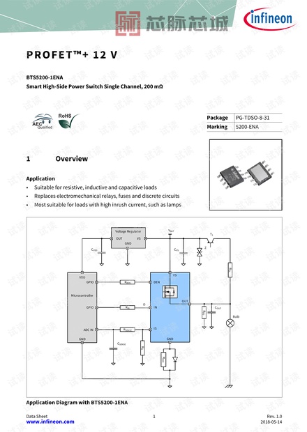
The BTS5200-1ENA is a 200 mΩ single channel Smart High-Side Power Switch, embedded in a PG-TDSO-8-31,
Exposed Pad package, providing protective functions and diagnosis. The power transistor is built by an
N-channel vertical power MOSFET with charge pump. The device is integrated in Smart6 technology. It is
specially designed to drive lamps up to 1x R10W 12V, as well as LEDs in the harsh automotive environment.
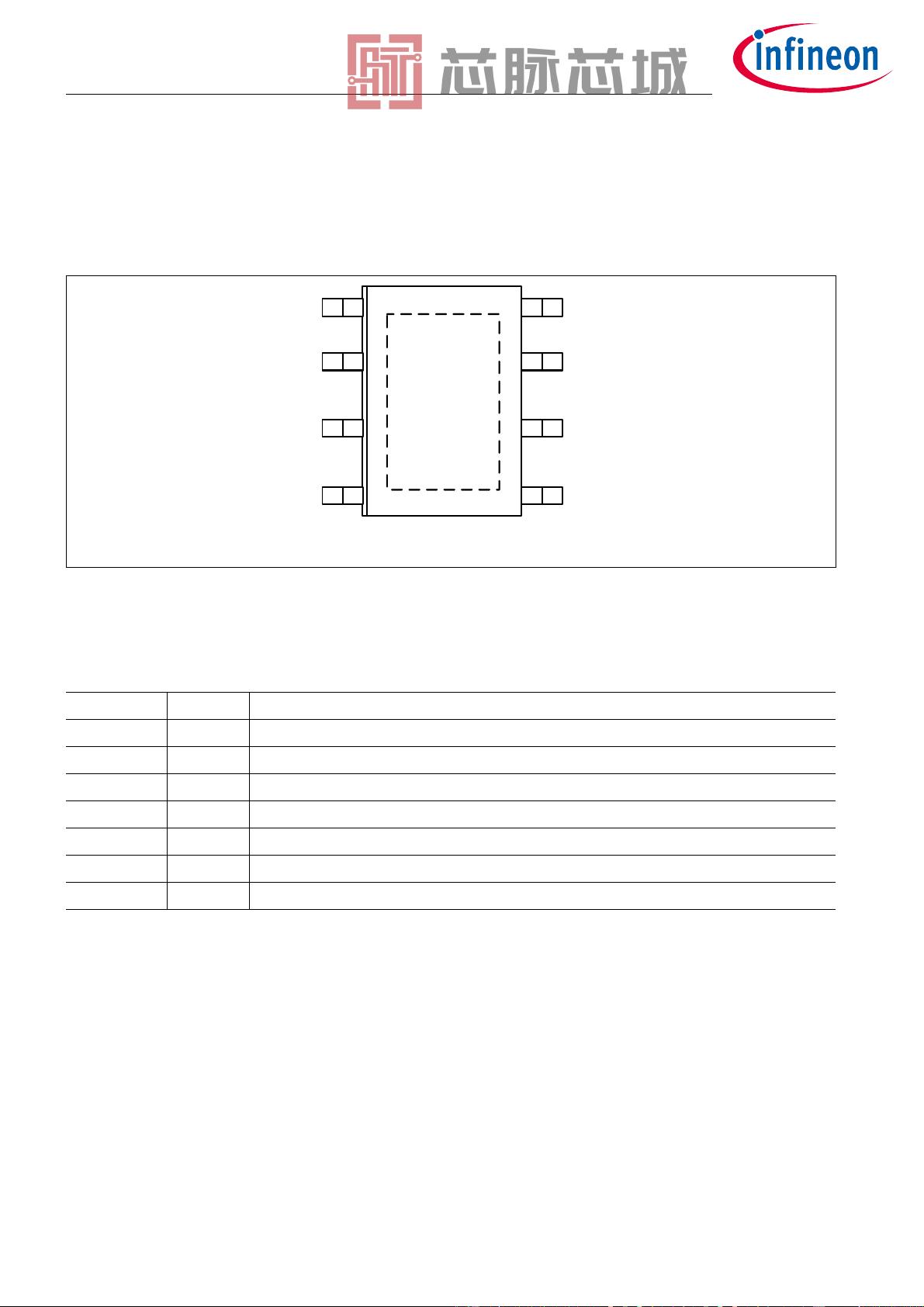
Diagnostic Functions
• Proportional load current sense
• Open load detection in ON and OFF
• Short circuit to battery and ground indication
• Overtemperature switch off detection
• Stable diagnostic signal during short circuit
•Enhanced k
ILIS
dependency with temperature and load current
Protection Functions
• Stable behavior during undervoltage
• Reverse polarity protection with external components
• Secure load turn-off during logic ground disconnection with external components
• Overtemperature protection with restart
• Overvoltage protection with external components
• Enhanced short circuit operation
Table 1 Product Summary
Parameter Symbol Value
Operating voltage range V
S(OP)
5 V ... 28 V
Maximum supply voltage V
S(LD)
41 V
Maximum ON state resistance at T
J
= 150°C R
DS(ON)
400 mΩ
Nominal load current I
L(NOM)
1.5 A
Typical current sense ratio k
ILIS
300
Minimum current limitation I
L5(SC)
9A
Maximum standby current with load at T
J
= 25°C I
S(OFF)
500 nA
Data Sheet 3 Rev. 1.0
2018-05-14
PROFET™+ 12 V
BTS5200-1ENA
Block Diagram
2 Block Diagram
Figure 1 Block Diagram for the BTS5200-1ENA
Block diagram.emf
VS
OUT
IN
T
driver
logic
gate control
&
charge p ump
load current sense and
open load detection
over
temperature
clamp for
ind uctiv e load
over current
switch limit
forwar d vol tage drop dete ction
voltage sen sor
GND
ESD
protection
IS
DEN
int ern al
power
supply
Data Sheet 4 Rev. 1.0
2018-05-14
PROFET™+ 12 V
BTS5200-1ENA
Pin Configuration
3 Pin Configuration
3.1 Pin Assignment
Figure 2 Pin Configuration
3.2 Pin Definitions and Functions
Table 2 Pin Definitions and Functions
Pin Symbol Function
1GNDGrouND; Ground connection
2ININput channel; Input signal for channel activation
3DENDiagnostic ENable; Digital signal to enable/disable the diagnosis of the device
4ISSense; Sense current of the selected channel
5NCNot Connected; No internal connection to the chip
6, 7, 8 OUT OUTput; Protected high side power output channel
1)
1) All output pins must be connected together on the PCB. All pins of the output are internally connected together. PCB
traces have to be designed to withstand the maximum current which can flow.
Cooling Tab VS Voltage Supply; Battery voltage
Pinout Single.vsd
OUT
OUT
OUT
GND
IN
DEN
IS NC
1
3
2
8
7
6
45
Data Sheet 5 Rev. 1.0
2018-05-14
PROFET™+ 12 V
BTS5200-1ENA
Pin Configuration
3.3 Voltage and Current Definition
Figure 3 shows all terms used in this data sheet, with associated convention for positive values.
Figure 3 Voltage and Current Definition
VS
IN
DEN
IS
GND
OUT
I
IN
I
DEN
I
IS
V
S
V
IN
V
DEN
V
IS
I
GND
V
DS
V
OUT
I
OUT
voltage an d curren t conven tio n single.vsd
I
VS
剩余44页未读,继续阅读
资源评论
芯脉芯城
- 粉丝: 3
- 资源: 4031
上传资源 快速赚钱
- 我的内容管理 展开
- 我的资源 快来上传第一个资源
- 我的收益 登录查看自己的收益
- 我的积分 登录查看自己的积分
- 我的C币 登录后查看C币余额
- 我的收藏
- 我的下载
- 下载帮助
安全验证
文档复制为VIP权益,开通VIP直接复制
信息提交成功