没有合适的资源?快使用搜索试试~ 我知道了~
ADM485EARZ-REEL7 ADI芯片 电子元器件中文版规格手册.pdf
需积分: 5 0 下载量 104 浏览量
2023-06-01
09:52:22
上传
评论
收藏 273KB PDF 举报
温馨提示
试读
17页
ADM485EARZ-REEL7 ADI芯片 电子元器件中文版规格手册
资源推荐
资源详情
资源评论
5 V, ±15 kV ESD Protected
Half-Duplex, RS-485/RS-422 Transceivers
ADM485E/ADM487E/ADM1487E
Rev. B
Information furnished by Analog Devices is believed to be accurate and reliable. However, no
responsibility is assumed by Analog Devices for its use, nor for any infringements of patents or other
rights of third parties that may result from its use. Specifications subject to change without notice. No
license is granted by implication or otherwise under any patent or patent rights of Analog Devices.
Trademarks and registered trademarks are the property of their respective owners.
One Technology Way, P.O. Box 9106, Norwood, MA 02062-9106, U.S.A.
Tel: 781.329.4700 www.analog.com
Fax: 781.461.3113 ©2007–2010 Analog Devices, Inc. All rights reserved.
FEATURES
TIA/EIA RS-485/RS-422 compliant
ESD protection on RS-485 I/O pins
±15 kV human body model (HBM)
Data rates
ADM487E: 250 kbps
ADM485E/ADM1487E: 2.5 Mbps
Half-duplex
Reduced slew rates for low EMI
Common-mode input range: −7 V to +12 V
Thermal shutdown and short-circuit protection
8-lead SOIC packages
ADM487EW qualified for automotive applications
APPLICATIONS
Energy/power metering
Lighting systems
Industrial control
Telecommunications
Security systems
Instrumentation
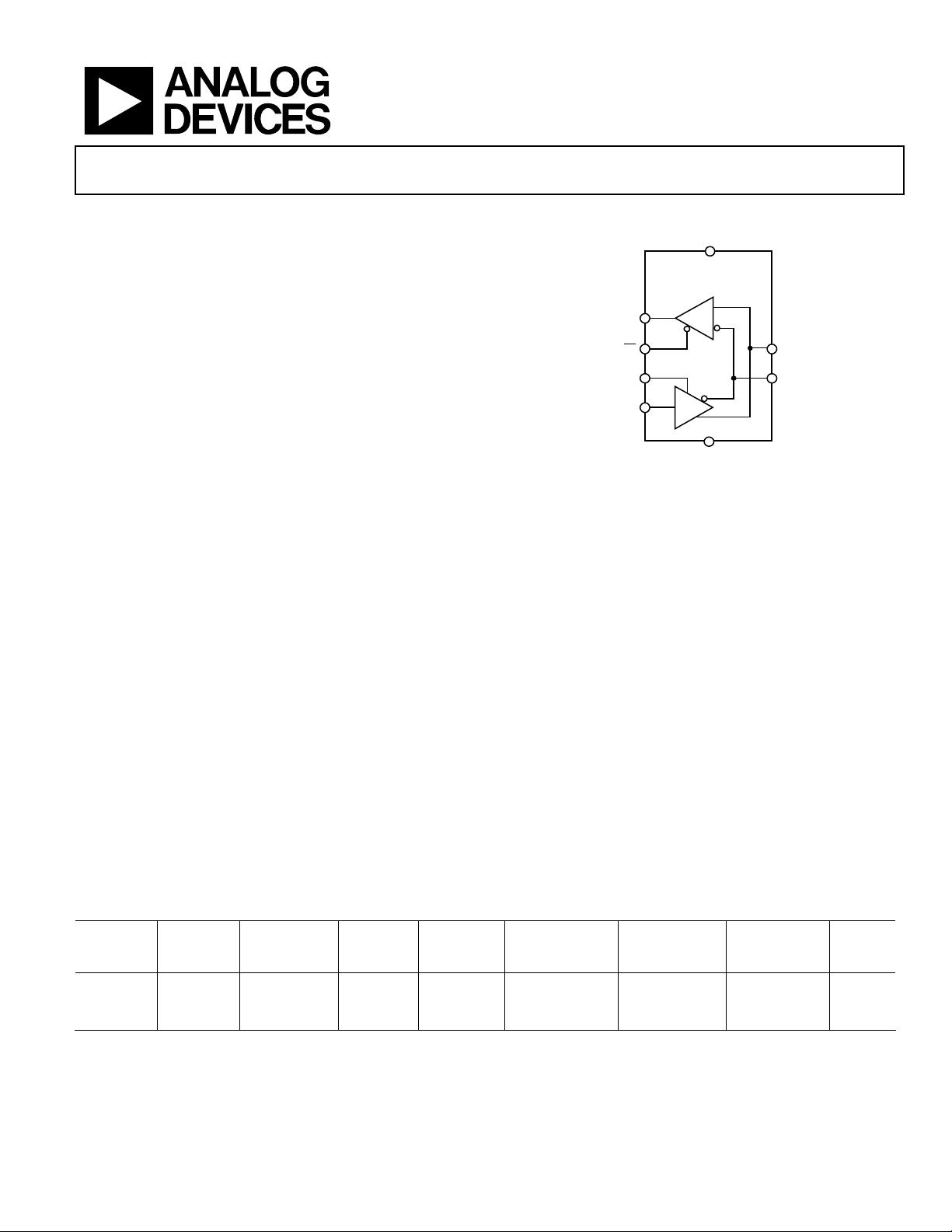
FUNCTIONAL BLOCK DIAGRAM
B
A
R
D
RO
RE
DE
DI
GND
V
CC
ADM485E/
ADM487E/
ADM1487E
06356-001
Figure 1.
GENERAL DESCRIPTION
The ADM485E/ADM487E/ADM1487E are 5 V, low power
data transceivers with ±15 kV ESD protection suitable for half-
duplex communication on multipoint bus transmission lines.
They are designed for balanced data transmission and comply
with Telecommunication Industry Association/Electronics
Industries Association (TIA/EIA) standards RS-485 and RS-422.
The ADM487E and ADM1487E have a 1/4 unit load receiver
input impedance that allows up to 128 transceivers on a bus,
whereas the ADM485E allows up to 32 transceivers on a bus.
Because only one driver is enabled at any time, the output of a
disabled or power-down driver is three-stated to avoid overloading
the bus.
The driver outputs are slew rate limited to reduce EMI and data
errors caused by reflections from improperly terminated buses.
Excessive power dissipation caused by bus contention or output
shorting is prevented with a thermal shutdown circuit.
The parts are fully specified over the industrial temperature
ranges and are available in 8-lead SOIC packages.
Table 1. Selection Table
Part
Number
Half-/Full-
Duplex
Guaranteed
Data Rate
(Mbps)
Slew Rate
Limited
Low Power
Shutdown
Driver/Receiver
Enable
Quiescent
Current (μA)
Number of
Nodes on Bus
Pin
Count
ADM485E Half 2.5 No No Yes 300 32 8
ADM487E Half 0.25 Yes Yes Yes 120 128 8
ADM1487E Half 2.5 No No Yes 230 128 8
ADM485E/ADM487E/ADM1487E
Rev. B | Page 2 of 16
TABLE OF CONTENTS
Features .............................................................................................. 1
Applications....................................................................................... 1
Functional Block Diagram .............................................................. 1
General Description......................................................................... 1
Revision History ............................................................................... 2
Specifications..................................................................................... 3
Timing Specifications .................................................................. 4
Absolute Maximum Ratings............................................................ 6
ESD Caution.................................................................................. 6
Pin Configuration and Function Descriptions............................. 7
Typical Performance Characteristics ..............................................8
Test Circuits and Switching Characteristics................................ 11
Theory of Operation ...................................................................... 13
Circuit Description .................................................................... 13
Applications Information.............................................................. 15
Differential Data Transmission ................................................ 15
Cable and Data Rate................................................................... 15
Outline Dimensions ....................................................................... 16
Ordering Guide .......................................................................... 16
Automotive Products................................................................. 16
REVISION HISTORY
10/10—Rev. A to Rev. B
Added ADM487EW Qualified for Automotive Applications to
Features Section ................................................................................ 1
Updated Outline Dimensions....................................................... 16
Changes to Ordering Guide .......................................................... 16
Added Automotive Products Section .......................................... 16
3/08—Rev. 0 to Rev. A
Changes to Supply Voltage Range ....................................Universal
Added Endnote 1 .............................................................................. 3
Changes to Table 3............................................................................ 4
Changes to Table 4............................................................................ 5
Changes to Figure 12........................................................................ 9
Changes to Figure 27 and Table 9................................................. 14
Changes to Figure 29...................................................................... 15
Updated Outline Dimensions....................................................... 16
1/07—Revision 0: Initial Version
ADM485E/ADM487E/ADM1487E
Rev. B | Page 3 of 16
SPECIFICATIONS
V
CC
= 5 V ± 10%, T
A
= T
MIN
to T
MAX
, unless otherwise noted.
Table 2. ADM485E/ADM487E/ADM1487E
Parameter Symbol Min Typ Max Unit Test Conditions/Comments
DRIVER
Differential Outputs
Differential Output Voltage (No Load) V
OD1
5 V
V
OD2
2 V R
L
= 50 Ω (RS-422) Differential Output Voltage (with Load)
1.5 5 V R
L
= 27 Ω (RS-485) (see Figure 18)
Δ |V
OD
| for Complementary Output States 0.2 V R
L
= 27 Ω or 50 Ω (see Figure 18)
Common-Mode Output Voltage V
OC
3 V R
L
= 27 Ω or 50 Ω (see Figure 18)
Δ |V
OC
| for Complementary Output States 0.2 V R
L
= 27 Ω or 50 Ω (see Figure 18)
Logic Inputs
Input High Voltage V
IH
2.0 V
DE, DI, RE
Input Low Voltage V
IL
0.8 V
DE, DI, RE
Logic Input Current
1
I
IN1
±2 μA
DE, DI, RE
RECEIVER
I
IN2
1.0 mA DE = 0 V, V
IN
= 12 V
−0.8 mA V
CC
= 0 V or 5.25 V, V
IN
= −7 V (ADM485E)
0.25 mA DE = 0 V, V
IN
= 12 V
Input Current (A, B)
−0.2 mA
V
CC
= 0 V or 5.25 V, V
IN
= −7 V
(ADM487E/ADM1487E)
Differential Inputs
Differential Input Threshold Voltage V
TH
−0.2 +0.2 V −7 V < V
CM
< +12 V
Input Hysteresis ΔV
TH
70 mV V
CM
= 0 V
Receiver Output Logic
Output Voltage High V
OH
3.5 V I
OUT
= −4 mA, V
ID
= +200 mV
Output Voltage Low V
OL
0.4 V I
OUT
= +4 mA, V
ID
= −200 mV
Three-State Output Leakage Current I
OZR
±1 μA 0.4 V < V
O
< 2.4 V
R
IN
12 kΩ −7 V < V
CM
< +12 V (ADM485E) Receiver Input Resistance
48 kΩ −7 V < V
CM
< +12 V (ADM487E/ADM1487E)
POWER SUPPLY
I
CC
500 900 μA
RE
= 0 V or V
CC
, DE = V
CC
(ADM485E)
300 500 μA
RE
= 0 V or V
CC
, DE = 0 V (ADM485E)
300 500 μA
RE
= 0 V or V
CC
, DE = V
CC
(ADM1487E)
230 400 μA
RE
= 0 V or V
CC
, DE = 0 V (ADM1487E)
250 400 μA
RE
= 0 V or V
CC
, DE = V
CC
(ADM487E)
No Load Supply Current
120 250 μA
RE
= 0 V, DE = 0 V (ADM487E)
Supply Current in Shutdown I
SHDN
0.5 10 μA
DE = 0 V, RE
= V
CC
(ADM487E)
Driver Short-Circuit Current, V
O
High I
OSD1
35 250 mA −7 V ≤ V
O
≤ +12 V, applies to peak current
Driver Short-Circuit Current, V
O
Low I
OSD2
35 250 mA −7 V ≤ V
O
≤ +12 V, applies to peak current
Receiver Short-Circuit Current I
OSR
7 95 mA 0 V ≤ V
O
≤ V
CC
ESD PROTECTION
A, B ±15 kV Human body model
1
Supply voltage is 5 V ± 5%.
剩余16页未读,继续阅读
资源评论
芯脉芯城
- 粉丝: 3
- 资源: 4031
上传资源 快速赚钱
- 我的内容管理 展开
- 我的资源 快来上传第一个资源
- 我的收益 登录查看自己的收益
- 我的积分 登录查看自己的积分
- 我的C币 登录后查看C币余额
- 我的收藏
- 我的下载
- 下载帮助
最新资源
- Screenshot_20240427_031602.jpg
- 网页PDF_2024年04月26日 23-46-14_QQ浏览器网页保存_QQ浏览器转格式(6).docx
- 直接插入排序,冒泡排序,直接选择排序.zip
- 在排序2的基础上,再次对快排进行优化,其次增加快排非递归,归并排序,归并排序非递归版.zip
- 实现了7种排序算法.三种复杂度排序.三种nlogn复杂度排序(堆排序,归并排序,快速排序)一种线性复杂度的排序.zip
- 冒泡排序 直接选择排序 直接插入排序 随机快速排序 归并排序 堆排序.zip
- 课设-内部排序算法比较 包括冒泡排序、直接插入排序、简单选择排序、快速排序、希尔排序、归并排序和堆排序.zip
- Python排序算法.zip
- C语言实现直接插入排序、希尔排序、选择排序、冒泡排序、堆排序、快速排序、归并排序、计数排序,并带图详解.zip
- 常用工具集参考用于图像等数据处理
资源上传下载、课程学习等过程中有任何疑问或建议,欢迎提出宝贵意见哦~我们会及时处理!
点击此处反馈
安全验证
文档复制为VIP权益,开通VIP直接复制
信息提交成功