IPTC019N10NM5 INFINEON 英飞凌芯片 中文版规格书手册.pdf
需积分: 5 6 浏览量
2023-06-01
09:51:52
上传
评论
收藏 1.4MB PDF 举报

1
IPTC019N10NM5
Rev.2.0,2021-02-02Final Data Sheet
1
8
9
16
8
1
9
16
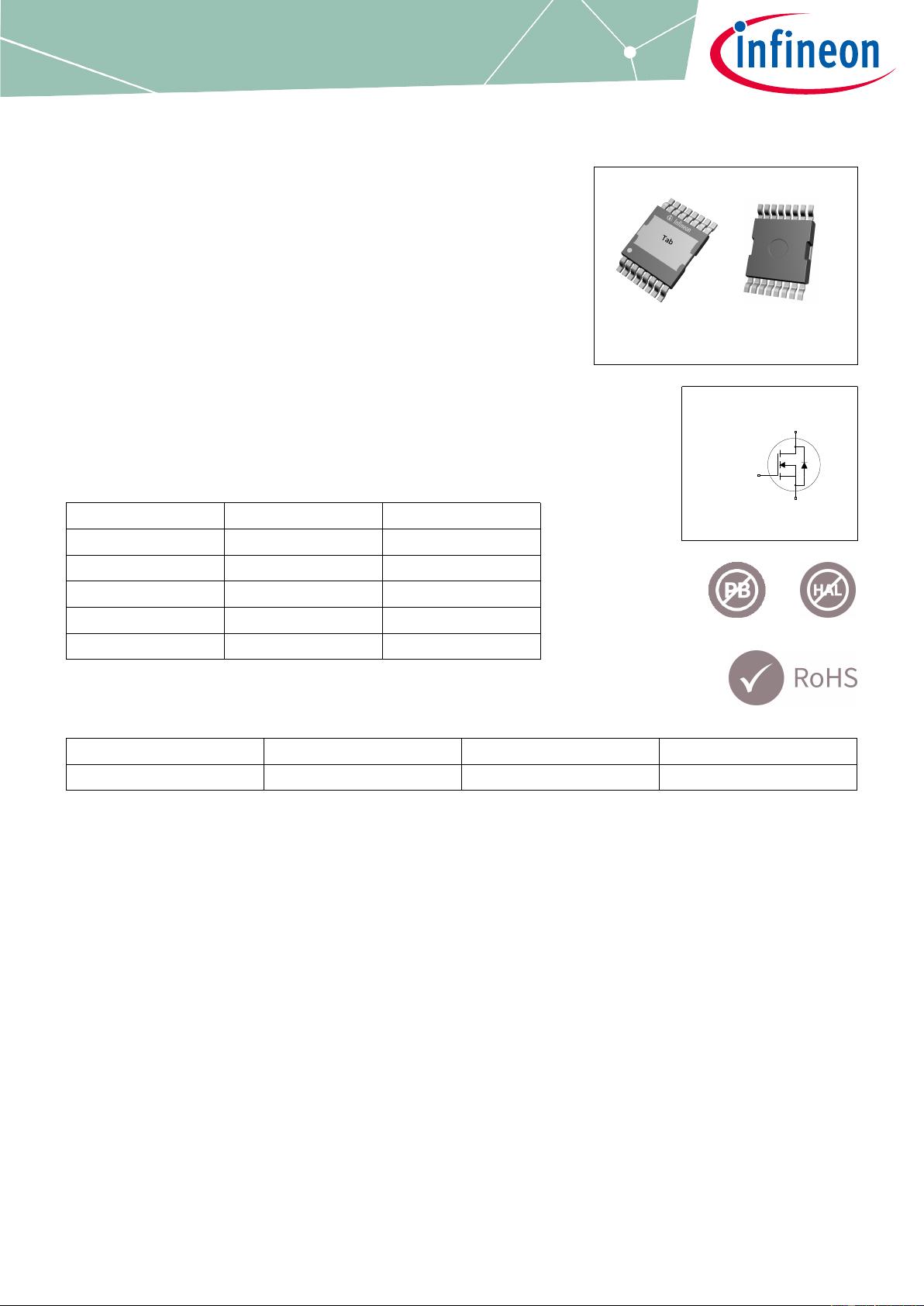
PG-HDSOP-16-2
Drain
Pin 9-16, Tab
Gate
Pin 8
Source
Pin 1-7
MOSFET
OptiMOS
TM
5Power-Transistor,100V
Features
•Optimizedformotordrivesandbatterypoweredapplications
•Optimizedfortopsidecooling
•Highcurrentcapability
•175°Crated
•100%avalanchetested
•Superiorthermalperformance
•N-channel
•Pb-freeleadplating;RoHScompliant
•Halogen-freeaccordingtoIEC61249-2-21
Productvalidation
FullyqualifiedaccordingtoJEDECforIndustrialApplications
Table1KeyPerformanceParameters
Parameter Value Unit
V
DS
100 V
R
DS(on),max
1.9 mΩ
I
D
279 A
Q
oss
163 nC
Q
G
128 nC
Type/OrderingCode Package Marking RelatedLinks
IPTC019N10NM5 PG-HDSOP-16 19N10NM5 -

剩余10页未读,继续阅读
资源评论


