没有合适的资源?快使用搜索试试~ 我知道了~
Precision, Micropower, Low-Dropout, High-Output-Current, SOT23 Voltage References
资源详情
资源评论
资源推荐
General Description
The MAX6061–MAX6067 are precision, low-dropout,
micropower voltage references. These three-terminal
devices operate with an input voltage range from (V
OUT
+ 50mV typ) to 12.6V and are available with output volt-
age options of 1.25V, 2.048V, 2.5V, 3V, 4.096V, 4.5V,
and 5V. They feature a proprietary curvature-correction
circuit and laser-trimmed thin-film resistors that result in a
very low temperature coefficient of 20ppm/°C (max) and
an initial accuracy of ±0.02% (max). Specifications apply
to the extended temperature range (-40°C to +85°C).
The MAX6061–MAX6067 typically draw only 90µA of
supply current and can source 5mA or sink 2mA of load
current. Unlike conventional shunt-mode (two-terminal)
references that waste supply current and require an
external resistor, these devices offer a supply current
that is virtually independent of the supply voltage
(8µA/V variation) and do not require an external resis-
tor. Additionally, the internally compensated devices do
not require an external compensation capacitor and are
stable with up to 1µF of load capacitance. Eliminating
the external compensation capacitor saves valuable
board area in space-critical applications. Low dropout
voltage and supply independent, ultra-low supply cur-
rent make these devices ideal for battery-operated,
high-performance, low-voltage systems.
The MAX6061–MAX6067 are available in a 3-pin SOT23
package.
Applications
Analog-to-Digital Converters (ADCs)
Portable Battery-Powered Systems
Notebook Computers
PDAs, GPS, DMMs
Cellular Phones
Precision 3V/5V Systems
Features
♦ Ultra-Small 3-Pin SOT23 Package
♦ ±0.2% max Initial Accuracy
♦ 20ppm/°C max Temperature Coefficient
♦ 5mA Source Current at 0.5mV/mA
♦ 2mA Sink Current at 1.3mV/mA
♦ Stable with C
LOAD
= 0 to 1µF
♦ 90µA typ Quiescent Supply Current
♦ 200mV max Dropout at 1mA Load Current
♦ +10µV/V Line Regulation
♦ Output Voltage Options: 1.25V, 2.048V, 2.5V, 3V,
4.096V, 4.5V, 5V
♦ 13µVp-p Noise 0.1Hz to 10Hz (MAX6061)
MAX6061–MAX6067
Precision, Micropower, Low-Dropout,
High-Output-Current, SOT23 Voltage References
________________________________________________________________ Maxim Integrated Products 1
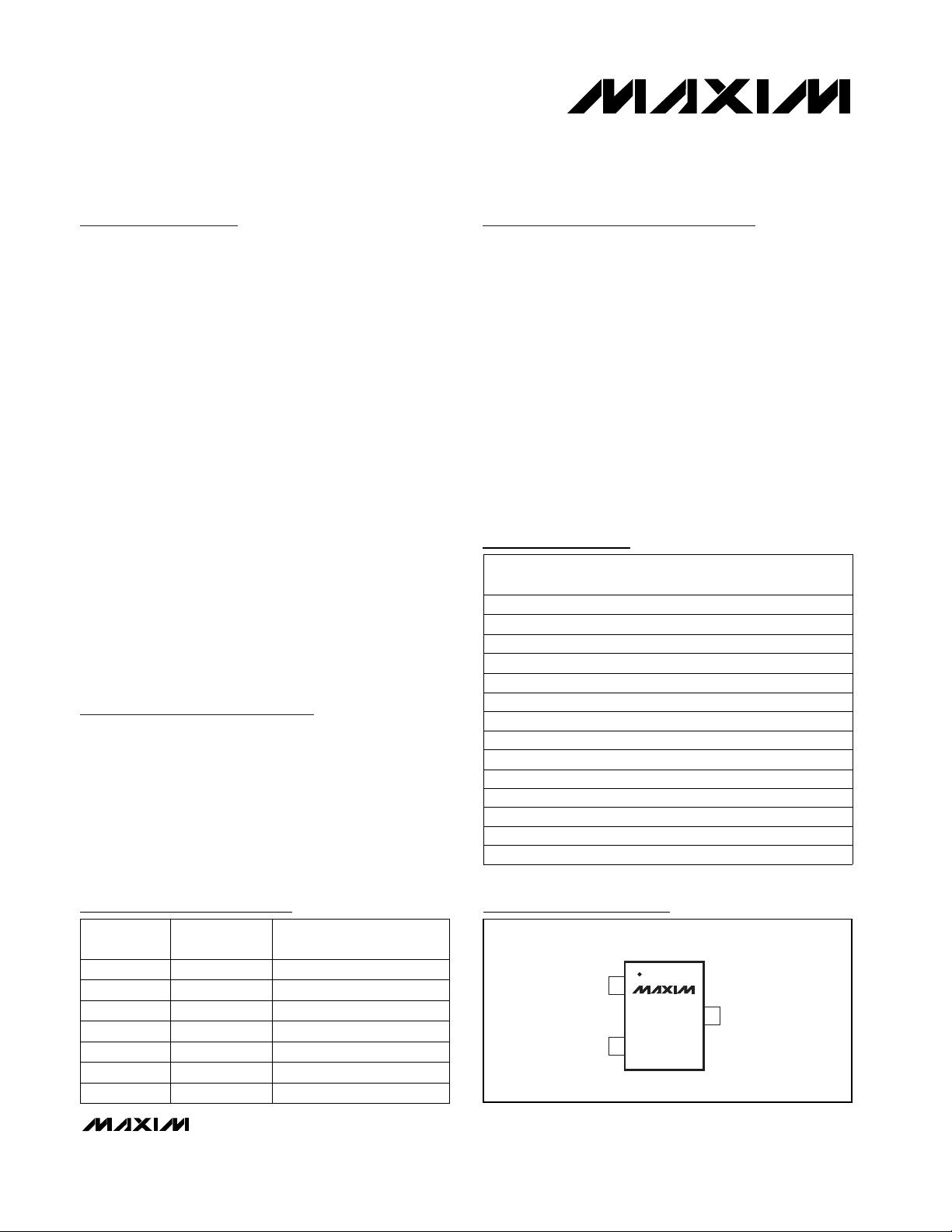
OUT
1
3 GND
IN
MAX6061–
MAX6067
SOT23-3
TOP VIEW
2
19-1659; Rev 0; 4/00
Ordering Information
Pin Configuration
Selector Guide
Note: There is a minimum order increment of 2500 pieces for
SOT packages.
For free samples and the latest literature, visit www.maxim-ic.com or phone 1-800-998-8800.
For small orders, phone 1-800-835-8769.
FZGC3 SOT23-3-40°C to +85°CMAX6064BEUR-T
FZGB3 SOT23-3-40°C to +85°C
MAX6064AEUR-T
FZFT3 SOT23-3-40°C to +85°CMAX6067BEUR-T
FZFS3 SOT23-3-40°C to +85°C
MAX6067AEUR-T
FZFN3 SOT23-3-40°C to +85°CMAX6066BEUR-T
FZFM3 SOT23-3-40°C to +85°C
MAX6066AEUR-T
FZGF
FZGE
3 SOT23-3
3 SOT23-3-40°C to +85°C
-40°C to +85°CMAX6065BEUR-T
MAX6065AEUR-T
FZFW
FZFV
FZFZ
3 SOT23-3
3 SOT23-3
3 SOT23-3-40°C to +85°C
-40°C to +85°C
-40°C to +85°CMAX6063BEUR-T
MAX6063AEUR-T
MAX6062BEUR-T
FZFY
FZFQ
FZFP
TOP
MARK
3 SOT23-3
3 SOT23-3
3 SOT23-3
PIN-
PACKAGE
TEMP. RANGE
-40°C to +85°C
-40°C to +85°C
-40°C to +85°C
MAX6062AEUR-T
MAX6061BEUR-T
MAX6061AEUR-T
PART
MAX6063 3.000 (V
OUT
+ 200mV) to 12.6
PART
OUTPUT
VOLTAGE (V)
INPUT VOLTAGE (V)
MAX6062
MAX6061 1.250 2.5 to 12.6
2.048 2.5 to 12.6
MAX6066 2.500 (V
OUT
+ 200mV) to 12.6
MAX6067
MAX6064 4.096 (V
OUT
+ 200mV) to 12.6
4.500 (V
OUT
+ 200mV) to 12.6
MAX6065 5.000 (V
OUT
+ 200mV) to 12.6
Typical Operating Circuit appears at end of data sheet.
MAX6061–MAX6067
Precision, Micropower, Low-Dropout,
High-Output-Current, SOT23 Voltage References
2 _______________________________________________________________________________________
ABSOLUTE MAXIMUM RATINGS
ELECTRICAL CHARACTERISTICS—MAX6061, V
OUT
= 1.25V
(V
IN
= +5V, I
OUT
= 0, T
A
= T
MIN
to T
MAX
, unless otherwise noted. Typical values are at T
A
= +25°C.) (Note 1)
Stresses beyond those listed under “Absolute Maximum Ratings” may cause permanent damage to the device. These are stress ratings only, and functional
operation of the device at these or any other conditions beyond those indicated in the operational sections of the specifications is not implied. Exposure to
absolute maximum rating conditions for extended periods may affect device reliability.
(Voltages Referenced to GND)
IN .........................................................................-0.3V to +13.5V
OUT .............................................................-0.3V to (V
IN
+ 0.3V)
Output Short-Circuit Duration to GND or IN (V
IN
< 6V)...Continuous
Output Short-Circuit Duration to GND or IN (V
IN
≥ 6V)................60s
Continuous Power Dissipation (T
A
= +70°C)
3-Pin SOT23 (derate 4.0mW/°C above +70°C)............320mW
Operating Temperature Range ...........................-40°C to +85°C
Storage Temperature Range .............................-65°C to +150°C
Lead Temperature (soldering, 10s) .................................+300°C
MAX6061A
MAX6061B
1.245 1.250 1.255
PARAMETER SYMBOL MIN TYP MAX UNITS
OUT Short-Circuit Current I
SC
25
mA
1.3 3.0
Load Regulation
∆V
OUT
/
∆I
OUT
0.5 0.9
mV/mA
Line Regulation
∆V
OUT
/
∆V
IN
10 250
µV/V
25
Long-Term Stability
∆V
OUT
/
time
62
ppm/
1000h
Output Voltage Hysteresis
(Note 3)
∆V
OUT
/
cycle
130
ppm
Output Voltage Temperature
Coefficient (Note 2)
Output Voltage V
OUT
1.243 1.250 1.257
V
TCV
OUT
620
ppm/°C
630
Noise Voltage e
OUT
13
µVp-p
15
µV
RMS
Ripple Rejection
∆V
OUT
/
∆V
IN
86
dB
Turn-On Settling Time t
R
50
µs
Capacitive-Load Stability Range
(Note 4)
C
OUT
0 1.0
µF
Supply Voltage Range V
IN
2.5 12.6
V
Quiescent Supply Current I
IN
90 125
µA
Change in Supply Current I
IN
/V
IN
3.4 8.0
µA/V
CONDITIONS
f = 0.1Hz to 10Hz
Short to GND
f = 10Hz to 10kHz
Sinking: -2mA ≤ I
OUT
≤ 0
Sourcing: 0 ≤ I
OUT
≤ 4mA
2.5V ≤ V
IN
≤ 12.6V
Short to IN
1000h at +25°C
V
IN
= 5V ±100mV, f = 120Hz
To V
OUT
= 0.1% of final value, C
OUT
= 50pF
Guaranteed by line-regulation test
T
A
= +25°C
MAX6061A
2.5V ≤ V
IN
≤ 12.6V
MAX6061B
DYNAMIC CHARACTERISTICS
INPUT CHARACTERISTICS
MAX6061–MAX6067
Precision, Micropower, Low-Dropout,
High-Output-Current, SOT23 Voltage References
_______________________________________________________________________________________ 3
ELECTRICAL CHARACTERISTICS—MAX6062, V
OUT
= 2.048V
(V
IN
= +5V, I
OUT
= 0, T
A
= T
MIN
to T
MAX
, unless otherwise noted. Typical values are at T
A
= +25°C.) (Note 1)
MAX6062B
MAX6062A
Output Voltage V
OUT
2.043 2.048 2.053
PARAMETER SYMBOL MIN TYP MAX UNITS
OUT Short-Circuit Current I
SC
25
mA
1.5 4
Load Regulation
∆V
OUT
/
∆I
OUT
0.5 0.9
mV/mA
Line Regulation
∆V
OUT
/
∆V
IN
33 130
µV/V
25
Long-Term Stability
∆V
OUT
/
time
62
ppm/
1000h
Output Voltage Hysteresis
(Note 3)
∆V
OUT
/
cycle
130
ppm
Output Voltage Temperature
Coefficient (Note 2)
2.040 2.048 2.056
TCV
OUT
620
ppm/°C
630
Noise Voltage e
OUT
22
µVp-p
25
µV
RMS
Ripple Rejection
∆V
OUT
/
∆V
IN
86
dB
Turn-On Settling Time t
R
115
µs
Capacitive-Load Stability Range
(Note 4)
C
OUT
0 1.0
µF
Supply Voltage Range V
IN
2.5 12.6
V
Quiescent Supply Current I
IN
90 125
µA
Change in Supply Current I
IN
/V
IN
3.3 8.0
µA/V
CONDITIONS
f = 0.1Hz to 10Hz
Short to GND
f = 10Hz to 10kHz
Sinking: -2mA ≤ I
OUT
≤ 0
Sourcing: 0 ≤ I
OUT
≤ 5mA
2.5V ≤ V
IN
≤ 12.6V
Short to IN
1000h at +25°C
V
IN
= 5V ±100mV, f = 120Hz
To V
OUT
= 0.1% of final value, C
OUT
= 50pF
(Note 2)
Guaranteed by line-regulation test
T
A
= +25°C
MAX6062A
2.5V ≤ V
IN
≤ 12.6V
MAX6062B
V
DYNAMIC CHARACTERISTICS
INPUT CHARACTERISTICS
MAX6061–MAX6067
Precision, Micropower, Low-Dropout,
High-Output-Current, SOT23 Voltage References
4 _______________________________________________________________________________________
ELECTRICAL CHARACTERISTICS—MAX6066, V
OUT
= 2.500V
(V
IN
= +5V, I
OUT
= 0, T
A
= T
MIN
to T
MAX
, unless otherwise noted. Typical values are at T
A
= +25°C.) (Note 1)
MAX6066B
MAX6066A
T
A
= +25°C V
2.495 2.500 2.505
V
OUT
Output Voltage
MAX6066B
(V
OUT
+ 0.2V) ≤ V
IN
≤ 12.6V
MAX6066A
Guaranteed by line-regulation test
To V
OUT
= 0.1% of final value, C
OUT
= 50pF
V
IN
= 5V ±100mV, f = 120Hz
1000h at +25°C
Short to IN
(V
OUT
+ 0.2V) ≤ V
IN
≤ 12.6V
Sourcing: 0 ≤ I
OUT
≤ 5mA
Sinking: -2mA ≤ I
OUT
≤ 0
f = 10Hz to 10kHz
Short to GND
f = 0.1Hz to 10Hz
CONDITIONS
µA/V
3.3 8.0
I
IN
/V
IN
Change in Supply Current
µA
90 125
I
IN
Quiescent Supply Current
V
V
OUT
+ 0.2 12.6
V
IN
Supply Voltage Range
µF
0 1.0
C
OUT
Capacitive-Load Stability Range
(Note 4)
µs
115
t
R
Turn-On Settling Time
dB
86
∆V
OUT
/
∆V
IN
Ripple Rejection
µV
RMS
30
µVp-p
27
e
OUT
Noise Voltage
630
ppm/°C
620
TCV
OUT
2.490 2.500 2.510
Output Voltage Temperature
Coefficient (Note 2)
ppm
130
∆V
OUT
/
cycle
Output Voltage Hysteresis
(Note 3)
ppm/
1000h
62
∆V
OUT
/
time
Long-Term Stability
25
µV/V
60 220
∆V
OUT
/
∆V
IN
Line Regulation
mV/mA
0.5 0.9
∆V
OUT
/
∆I
OUT
Load Regulation
1.6 5
mA
25
I
SC
OUT Short-Circuit Current
UNITSMIN TYP MAXSYMBOLPARAMETER
I
OUT
= 1mA mV
50 200
V
IN
-
V
OUT
Dropout Voltage (Note 5)
DYNAMIC CHARACTERISTICS
INPUT CHARACTERISTICS
剩余15页未读,继续阅读
wzw1103
- 粉丝: 1
- 资源: 8
上传资源 快速赚钱
- 我的内容管理 展开
- 我的资源 快来上传第一个资源
- 我的收益 登录查看自己的收益
- 我的积分 登录查看自己的积分
- 我的C币 登录后查看C币余额
- 我的收藏
- 我的下载
- 下载帮助
安全验证
文档复制为VIP权益,开通VIP直接复制
信息提交成功
评论0