没有合适的资源?快使用搜索试试~ 我知道了~
MAX1978-1979
1星 需积分: 50 17 下载量 200 浏览量
2012-09-19
21:08:04
上传
评论
收藏 618KB PDF 举报
温馨提示
试读
20页
详细描叙MAX1978-1979的内部电路,接口属性,对于充分了解MAX1978-1979很有帮助。
资源推荐
资源详情
资源评论
General Description
The MAX1978/MAX1979 are the smallest, safest, most
accurate complete single-chip temperature controllers for
Peltier thermoelectric cooler (TEC) modules. On-chip power
FETs and thermal control-loop circuitry minimize external
components while maintaining high efficiency. Selectable
500kHz/1MHz switching frequency and a unique ripple-can-
cellation scheme optimize component size and efficiency
while reducing noise. Switching speeds of internal
MOSFETs are optimized to reduce noise and EMI. An ultra-
low-drift chopper amplifier maintains ±0.001°C temperature
stability. Output current, rather than voltage, is directly con-
trolled to eliminate current surges. Individual heating and
cooling current and voltage limits provide the highest level of
TEC protection.
The MAX1978 operates from a single supply and provides
bipolar ±3A output by biasing the TEC between the outputs
of two synchronous buck regulators. True bipolar operation
controls temperature without “dead zones” or other nonlin-
earities at low load currents. The control system does not
hunt when the set point is very close to the natural operating
point, where only a small amount of heating or cooling is
needed. An analog control signal precisely sets the TEC
current. The MAX1979 provides unipolar output up to 6A.
A chopper-stabilized instrumentation amplifier and a high-
precision integrator amplifier are supplied to create a pro-
portional-integral (PI) or proportional-integral-derivative (PID)
controller. The instrumentation amplifier can interface to an
external NTC or PTC thermistor, thermocouple, or semicon-
ductor temperature sensor. Analog outputs are provided to
monitor TEC temperature and current. In addition, separate
overtemperature and undertemperature outputs indicate
when the TEC temperature is out of range. An on-chip volt-
age reference provides bias for a thermistor bridge.
The MAX1978/MAX1979 are available in a low-profile
48-lead thin QFN-EP package and is specified over the
-40°C to +85°C temperature range. The thermally
enhanced QFN-EP package with exposed metal pad
minimizes operating junction temperature. An evaluation
kit is available to speed designs.
Applications
Fiber Optic Laser Modules
WDM, DWDM Laser-Diode Temperature Control
Fiber Optic Network Equipment
EDFA Optical Amplifiers
Telecom Fiber Interfaces
ATE
Features
♦ Smallest, Safest, Most Accurate Complete
Single-Chip Controller
♦ On-Chip Power MOSFETS—No External FETs
♦ Circuit Footprint < 0.93in
2
♦ Circuit Height < 3mm
♦ Temperature Stability to 0.001°C
♦ Integrated Precision Integrator and Chopper
Stabilized Op Amps
♦ Accurate, Independent Heating and Cooling
Current Limits
♦ Eliminates Surges By Directly Controlling
TEC Current
♦ Adjustable Differential TEC Voltage Limit
♦ Low-Ripple and Low-Noise Design
♦ TEC Current Monitor
♦ Temperature Monitor
♦ Over- and Undertemperature Alarm
♦ Bipolar ±3A Output Current (MAX1978)
♦ Unipolar +6A Output Current (MAX1979)
MAX1978/MAX1979
Integrated Temperature
Controllers for Peltier Modules
________________________________________________________________ Maxim Integrated Products 1
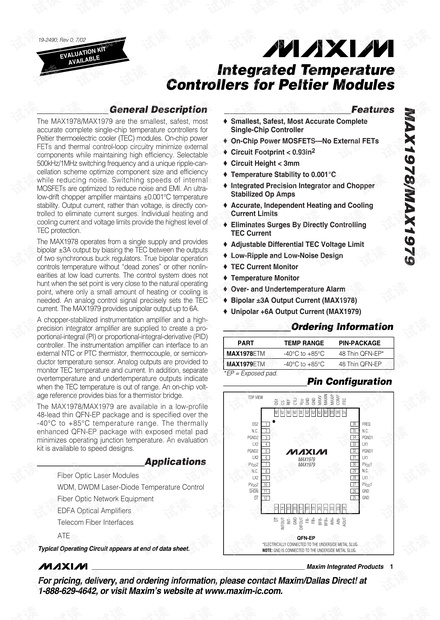
Ordering Information
FREQ
N.C.
LX1
PGND1
N.C.
LX1
PV
DD
1
GND
GND
LX1
PV
DD
1
PGND1
PGND2
LX2
PGND2
LX2
PV
DD
2
N.C.
LX2
N.C.
OS2
1
2
3
4
5
6
7
8
9
10
11
12
36
35
34
33
32
31
30
29
28
27
26
25
DIFOUT
FB-
FB+
BFB+
AOUT
AIN-
AIN+
GND
INT-
INTOUT
CS
REF
CTLI
V
DD
GND
GND
MAXV
MAXIN
MAXIP
ITEC
COMP
OS1
QFN-EP
MAX1978
MAX1979
BFB-
TOP VIEW
*ELECTRICALLY CONNECTED TO THE UNDERSIDE METAL SLUG.
NOTE: GND IS CONNECTED TO THE UNDERSIDE METAL SLUG.
48
47
46
45
44
43
42
41
40
39
38
37
13
14
15
16
17
18
19
20
21
22
23
24
OT
PV
DD
2
SHDN
UT
Pin Configuration
19-2490; Rev 0; 7/02
For pricing, delivery, and ordering information, please contact Maxim/Dallas Direct! at
1-888-629-4642, or visit Maxim’s website at www.maxim-ic.com.
Typical Operating Circuit appears at end of data sheet.
EVALUATION KIT
AVAILABLE
PART TEMP RANGE PIN-PACKAGE
MAX1978ETM -40°C to +85°C 48 Thin QFN-EP*
MAX1979ETM -40°C to +85°C 48 Thin QFN-EP
*EP = Exposed pad.
MAX1978/MAX1979
Integrated Temperature
Controllers for Peltier Modules
2 _______________________________________________________________________________________
ABSOLUTE MAXIMUM RATINGS
ELECTRICAL CHARACTERISTICS
(V
DD
= PV
DD
1 = PV
DD
2 = SHDN = 5V, FREQ = GND, CTLI = FB+ = FB- = MAXV = MAXIP = MAXIN = REF, T
A
= 0°C to +85°C,
unless otherwise noted. Typical values at T
A
= +25°C.)
Stresses beyond those listed under “Absolute Maximum Ratings” may cause permanent damage to the device. These are stress ratings only, and functional
operation of the device at these or any other conditions beyond those indicated in the operational sections of the specifications is not implied. Exposure to
absolute maximum rating conditions for extended periods may affect device reliability.
V
DD
to GND..............................................................-0.3V to +6V
SHDN, MAXV, MAXIP, MAXIN,
CTLI, OT, UT to GND............................................-0.3V to +6V
FREQ, COMP, OS1, OS2, CS, REF, ITEC, AIN+, AIN-,
AOUT, INT-, INTOUT, BFB+, BFB-, FB+, FB-,
DIFOUT to GND......................................-0.3V to (V
DD
+ 0.3V)
PV
DD
1, PV
DD
2 to V
DD
...........................................-0.3V to +0.3V
PV
DD
1, PV
DD
2 to GND...............................-0.3V to (V
DD
+ 0.3V)
PGND1, PGND2 to GND .......................................-0.3V to +0.3V
COMP, REF, ITEC, OT, UT, INTOUT, DIFOUT,
BFB-, BFB+, AOUT Short to GND .............................Indefinite
Peak LX Current (MAX1978) (Note 1).................................±4.5A
Peak LX Current (MAX1979) (Note 1)....................................+9A
Continuous Power Dissipation (T
A
= +70°C)
48-Lead Thin QFN-EP
(derate 26.3mW/°C above +70°C) (Note 2).................2.105W
Operating Temperature Ranges
MAX1978ETM ..................................................-40°C to +85°C
MAX1979ETM ..................................................-40°C to +85°C
Maximum Junction Temperature .....................................+150°C
Storage Temperature Range .............................-65°C to +150°C
Lead Temperature (soldering, 10s) .................................+300°C
PARAMETER SYMBOL CONDITIONS MIN TYP MAX UNITS
Input Supply Range V
DD
3.0 5.5 V
V
DD
= 5V, I
TEC
= 0 to ±3A,
V
OUT
= V
OS1
- V
OS2
(MAX1978)
-4.3 +4.3
V
DD
= 5V, I
TEC
= 0 to 6A,
V
OUT
= V
OS1
(MAX1979)
4.3
V
DD
= 3V, I
TEC
= 0 to ±3A,
V
OUT
= V
OS1
- V
OS2
(MAX1978)
-2.3 +2.3
Output Voltage Range V
OUT
V
DD
= 3V, I
TEC
= 0 to 6A,
V
OUT
= V
OS1
(MAX1979)
2.3
V
MAX1978 ±3
Maximum TEC Current I
TEC
(
MAX
)
MAX1979 6
A
Reference Voltage V
REF
V
DD
= 3V to 5.5V, I
REF
= 150µA 1.485 1.500 1.515 V
Reference Load Regulation ∆V
REF
V
DD
= 3V to 5.5V, I
REF
= +10µA to -1mA 1.2 5 mV
V
MAXI_
= V
REF
135 150 160
V
OS1
< V
CS
V
MAXI_
= V
REF
/3 40 50 60
V
MAXI_
= V
REF
135 150 160
Current-Sense Threshold
V
OS1
> V
CS
V
MAXI_
= V
REF
/3 40 50 60
mV
V
DD
= 5V, I = 0.5A 0.04 0.07
NFET On-Resistance R
DS
(
ON-N
)
V
DD
= 3V, I = 0.5A 0.06 0.08
Ω
V
DD
= 5V, I = 0.5A 0.06 0.10
PFET On-Resistance R
DS
(
ON-P
)
V
DD
= 3V, I = 0.5A 0.09 0.12
Ω
V
LX
= V
DD
= 5V, T
A
= +25°C 0.02 10
NFET Leakage I
LEAK
(
N
)
V
LX
= V
DD
= 5V, T
A
= +85°C1
µA
Note 1: LX has internal clamp diodes to PGND and PVDD. Applications that forward bias these diodes should not exceed the IC’s
package power dissipation limits.
Note 2: Solder underside metal slug to PC board ground plane.
MAX1978/MAX1979
Integrated Temperature
Controllers for Peltier Modules
_______________________________________________________________________________________ 3
ELECTRICAL CHARACTERISTICS (continued)
(V
DD
= PV
DD
1 = PV
DD
2 = SHDN = 5V, FREQ = GND, CTLI = FB+ = FB- = MAXV = MAXIP = MAXIN = REF, T
A
= 0°C to +85°C,
unless otherwise noted. Typical values at T
A
= +25°C.)
PARAMETER SYMBOL CONDITIONS MIN TYP MAX UNITS
V
LX
= 0, T
A
= +25°C 0.02 10
PFET Leakage I
LEAK(P)
V
LX
= 0, T
A
= +85°C1
µA
V
DD
= 5V 30 50
No-Load Supply Current
I
DD(NO
LOAD)
V
DD
= 3.3V 15 30
mA
Shutdown Supply Current I
DD-SD
SHDN = GND, V
DD
= 5V (Note 3) 2 3 mA
Thermal Shutdown T
S H U TD OWN
Hysteresis = 15°C 165 °C
V
DD
rising 2.4 2.6 2.8
UVLO Threshold V
UVLO
V
DD
falling 2.25 2.5 2.75
V
FREQ = GND 450 500 650
Switching Frequency Internal
Oscillator
f
SW-INT
FREQ=V
DD
800 1000 1200
kHz
OS1, OS2, CS Input Current
I
OS1
, I
OS2
,
I
CS
0 or V
DD
-100 +100 µA
SHDN, FREQ Input Current
I
SHDN
,
I
FREQ
0 or V
DD
-5 +5 µA
SHDN, FREQ Input Low Voltage V
IL
V
DD
= 3V to 5.5V
0.25 ×
V
DD
V
SHDN, FREQ Input High Voltage V
IH
V
DD
= 3V to 5.5V
0.75 ×
V
DD
V
V
MAXV
= V
REF
✕
0.67,
V
OS1
to V
OS2
= ±4V, V
DD
= 5V
-1 +1
MAXV Threshold Accuracy
V
MAXV
= V
REF
✕
0.33,
V
OS1
to V
OS2
= ±2V, V
DD
= 3V
-2 +2
%
MAXV, MAXIP, MAXIN
Input Bias Current
I
MAXV-BIAS
,
I
MAXI_-BIAS
V
MAXV
= V
MAXI_
= 0.1V or 1.5V -0.1 +0.1 µA
CTLI Gain A
CTLI
V
CTLI
= 0.5V to 2.5V (Note 4) 9.5 10 10.5 V/V
CTLI Input Resistance R
CTLI
1MΩ terminated at REF 0.5 1.0 2.0 MΩ
Error Amp Transconductance g
m
50 100 175 µS
ITEC Accuracy V
OS1
to V
CS
= +100mV or -100mV -10 +10 %
ITEC Load Regulation ∆V
ITEC
V
OS1
to V
CS
= +100mV or -100mV,
I
ITEC
= ±10µA
-0.1 +0.1 %
Instrumentation Amp Input Bias
Current
I
DIF-BIAS
-10 0 +10 nA
Instrumentation Amp Offset
Voltage
V
DIF-OS
V
DD
= 3V to 5.5V -200 +20 +200 µV
Instrumentation Amp Offset-
Voltage Drift with Temperature
V
DD
= 3V to 5.5V 0.1 µV/°C
Instrumentation Amp Preset
Gain
A
DIF
R
LOAD
= 10kΩ to REF 45 50 55 V/V
MAX1978/MAX1979
Integrated Temperature
Controllers for Peltier Modules
4 _______________________________________________________________________________________
ELECTRICAL CHARACTERISTICS (continued)
(V
DD
= PV
DD
1 = PV
DD
2 = SHDN = 5V, FREQ = GND, CTLI = FB+ = FB- = MAXV = MAXIP = MAXIN = REF, T
A
= 0°C to +85°C,
unless otherwise noted. Typical values at T
A
= +25°C.)
PARAMETER SYMBOL CONDITIONS MIN TYP MAX UNITS
Integrator Amp Open-Loop Gain A
OL-INT
R
LOAD
= 10kΩ to REF 120 dB
Integrator Amp CMRR CMRR
INT
100 dB
Integrator Amp Input Bias Current I
INT-BIAS
V
DD
= 3V to 5.5V 1 nA
Integrator Amp Voltage Offset V
INT-OS
V
DD
= 3V to 5.5V -3 +0.1 +3 mV
Integrator Amp Gain Bandwidth GBW
INT
100 kHz
Undedicated Chopper Amp
Open-Loop Gain
A
OL-AIN
R
LOAD
= 10kΩ to REF 120 dB
Undedicated Chopper Amp
CMRR
CMRR
AIN
85 dB
Undedicated Chopper Amp Input
Bias Current
I
AIN-BIAS
V
DD
= 3V to 5.5V -10 0 +10 nA
Undedicated Chopper Amp
Offset Voltage
V
AIN-OS
V
DD
= 3V to 5.5V -200 +10 +200 µV
Undedicated Chopper Amp Gain
Bandwidth
GBW
AIN
100 kHz
Undedicated Chopper Amp
Output Ripple
V
RIPPLE
A = 5 20 mV
BFB_ Buffer Error C
L OA D
< 100p F -200 0 +200 µV
UT and OT Leakage Current I
LEAK
V
UT
= V
OT
= 5.5V 1 µA
UT and OT Output Low Voltage V
OL
Sinking 4mA 50 150 mV
UT Trip Threshold FB+ - FB- (see Typical Application Circuit) -20 mV
OT Trip Threshold FB+ - FB- (see Typical Application Circuit)20 mV
剩余19页未读,继续阅读
资源评论
- doudou_zhu_2020-08-08就是数据手册,还以为是啥自己分析的东西呢,垃圾
taojun7816
- 粉丝: 0
- 资源: 3
上传资源 快速赚钱
- 我的内容管理 展开
- 我的资源 快来上传第一个资源
- 我的收益 登录查看自己的收益
- 我的积分 登录查看自己的积分
- 我的C币 登录后查看C币余额
- 我的收藏
- 我的下载
- 下载帮助
安全验证
文档复制为VIP权益,开通VIP直接复制
信息提交成功