没有合适的资源?快使用搜索试试~ 我知道了~
资源推荐
资源详情
资源评论
TPS7301Q, TPS7325Q, TPS7330Q, TPS7333Q, TPS7348Q, TPS7350Q
LOW-DROPOUT VOLTAGE REGULATORS
WITH INTEGRATED DELAYED RESET FUNCTION
SLVS124F – JUNE 1995 – REVISED JANUARY 1999
1
POST OFFICE BOX 655303 • DALLAS, TEXAS 75265
D
Available in 2.5-V, 3-V, 3.3-V, 4.85-V, and 5-V
Fixed-Output and Adjustable Versions
D
Integrated Precision Supply-Voltage
Supervisor Monitoring Regulator Output
Voltage
D
Active-Low Reset Signal with 200-ms Pulse
Width
D
Very Low Dropout Voltage ...Maximum of
35 mV at I
O
= 100 mA (TPS7350)
D
Low Quiescent Current – Independent of
Load . . . 340 µA Typ
D
Extremely Low Sleep-State Current,
0.5 µA Max
D
2% Tolerance Over Full Range of Load,
Line, and Temperature for Fixed-Output
Versions
§
D
Output Current Range of 0 mA to 500 mA
D
TSSOP Package Option Offers Reduced
Component Height For Critical Applications
description
The TPS73xx devices are members of a family of
micropower low-dropout (LDO) voltage regulators.
They are differentiated from the TPS71xx and TPS72xx LDOs by their integrated delayed microprocessor-reset
function. If the precision delayed reset is not required, the TPS71xx and TPS72xx should be considered.
¶
AVAILABLE OPTIONS
OUTPUT VOLTAGE
(V)
NEGATIVE-GOING RESET
THRESHOLD VOLTAGE (V)
PACKAGED DEVICES
CHIP FORM
T
J
MIN TYP MAX MIN TYP MAX
SMALL
OUTLINE
(D)
PLASTIC DIP
(P)
TSSOP
(PW)
CHIP
FORM
(Y)
4.9 5 5.1 4.55 4.65 4.75 TPS7350QD TPS7350QP TPS7350QPW TPS7350Y
4.75 4.85 4.95 4.5 4.6 4.7 TPS7348QD TPS7348QP TPS7348QPW TPS7348Y
40
°
Cto
3.23 3.3 3.37 2.868 2.934 3 TPS7333QD TPS7333QP TPS7333QPW TPS7333Y
–
40°C
to
125°C
2.94 3 3.06 2.58 2.64 2.7 TPS7330QD TPS7330QP TPS7330QPW TPS7330Y
125 C
2.425 2.5 2.575 2.23 2.32 2.39 TPS7325QD TPS7325QP TPS7325QPW TPS7325Y
Adjustable
1.2 V to 9.75 V
1.101 1.123 1.145 TPS7301QD TPS7301QP TPS7301QPW TPS7301Y
The D and PW packages are available taped and reeled. Add an R suffix to device type (e.g., TPS7350QDR). The TPS7301Q is programmable
using an external resistor divider (see application information). The chip form is tested at 25°C.
§
The TPS7325 has a tolerance of ±3% over the full temperature range.
¶
The TPS71xx and the TPS72xx are 500-mA and 250-mA output regulators respectively, offering performance similar to that of the TPS73xx but
without the delayed-reset function. The TPS72xx devices are further differentiated by availability in 8-pin thin-shrink small-outline packages
(TSSOP) for applications requiring minimum package size.
Please be aware that an important notice concerning availability, standard warranty, and use in critical applications of
Texas Instruments semiconductor products and disclaimers thereto appears at the end of this data sheet.
Copyright 1999, Texas Instruments Incorporated
PRODUCTION DATA information is current as of publication date.
Products conform to specifications per the terms of Texas Instruments
standard warranty. Production processing does not necessarily include
testing of all parameters.
1
2
3
4
5
6
7
8
9
10
20
19
18
17
16
15
14
13
12
11
GND
GND
GND
NC
NC
EN
NC
IN
IN
IN
RESET
NC
NC
FB
‡
NC
SENSE
†
OUT
OUT
NC
NC
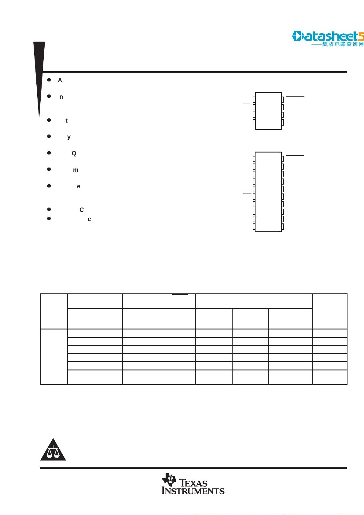
PW PACKAGE
(TOP VIEW)
NC – No internal connection
†
SENSE – Fixed voltage options only
(TPS7325, TPS7330, TPS7333, TPS7348, and TPS7350)
‡
FB – Adjustable version only (TPS7301)
1
2
3
4
8
7
6
5
GND
EN
IN
IN
RESET
SENSE
†
/FB
‡
OUT
OUT
D OR P PACKAGE
(TOP VIEW)
TPS7301Q, TPS7325Q, TPS7330Q, TPS7333Q, TPS7348Q, TPS7350Q
LOW-DROPOUT VOLTAGE REGULATORS
WITH INTEGRATED DELAYED RESET FUNCTION
SLVS124F – JUNE 1995 – REVISED JANUARY 1999
2
POST OFFICE BOX 655303 • DALLAS, TEXAS 75265
description (continued)
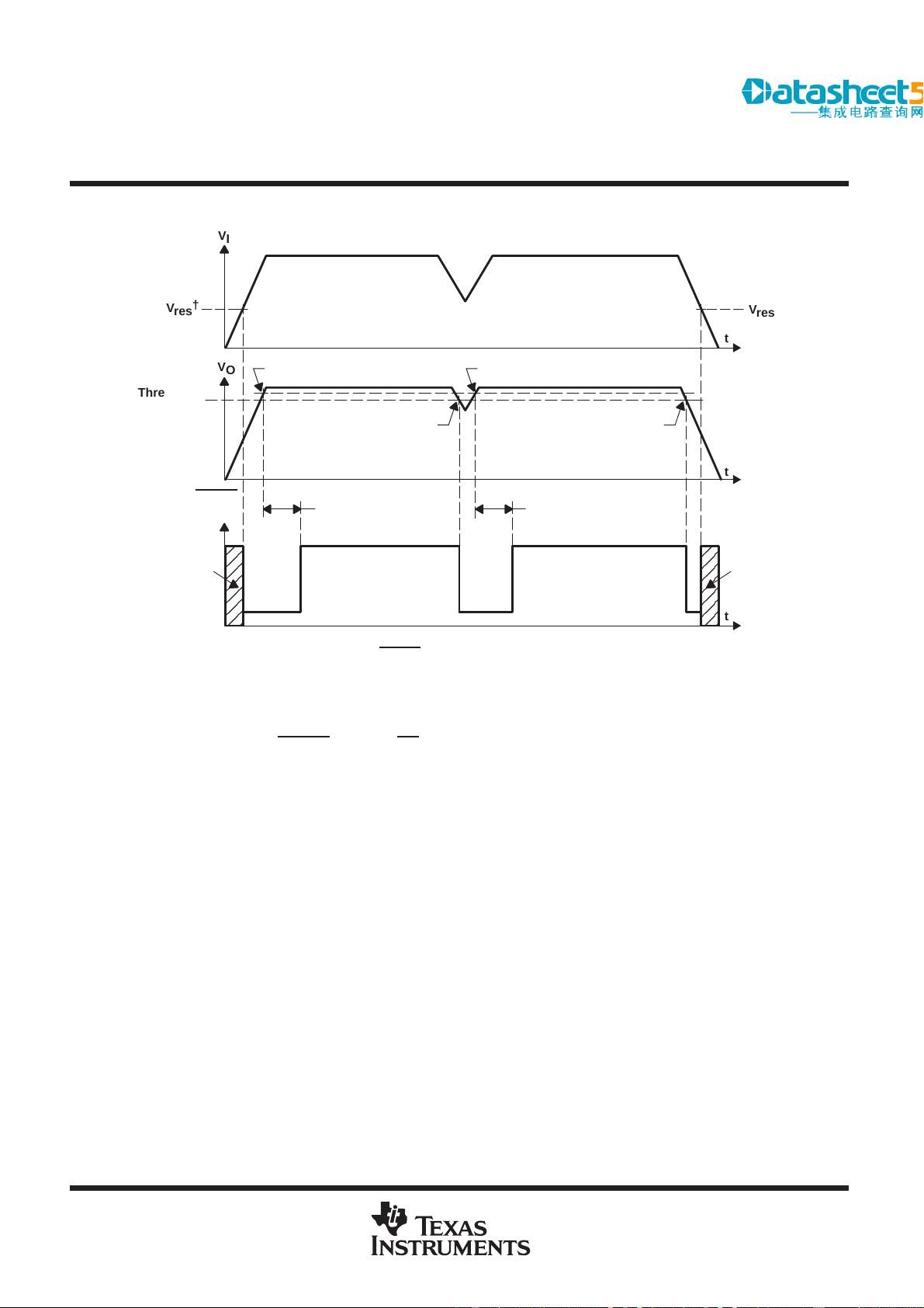
The RESET output of the TPS73xx initiates a reset in microcomputer and microprocessor systems in the event
of an undervoltage condition. An internal comparator in the TPS73xx monitors the output voltage of the regulator
to detect an undervoltage condition on the regulated output voltage.
If that occurs, the RESET output (open-drain NMOS) turns on, taking the RESET signal low. RESET stays low
for the duration of the undervoltage condition. Once the undervoltage condition ceases, a 200-ms (typ) time-out
begins. At the completion of the 200-ms delay, RESET
goes high.
An order of magnitude reduction in dropout voltage and quiescent current over conventional LDO performance
is achieved by replacing the typical pnp pass transistor with a PMOS device.
Because the PMOS device behaves as a low-value resistor, the dropout voltage is very low (maximum of 35 mV
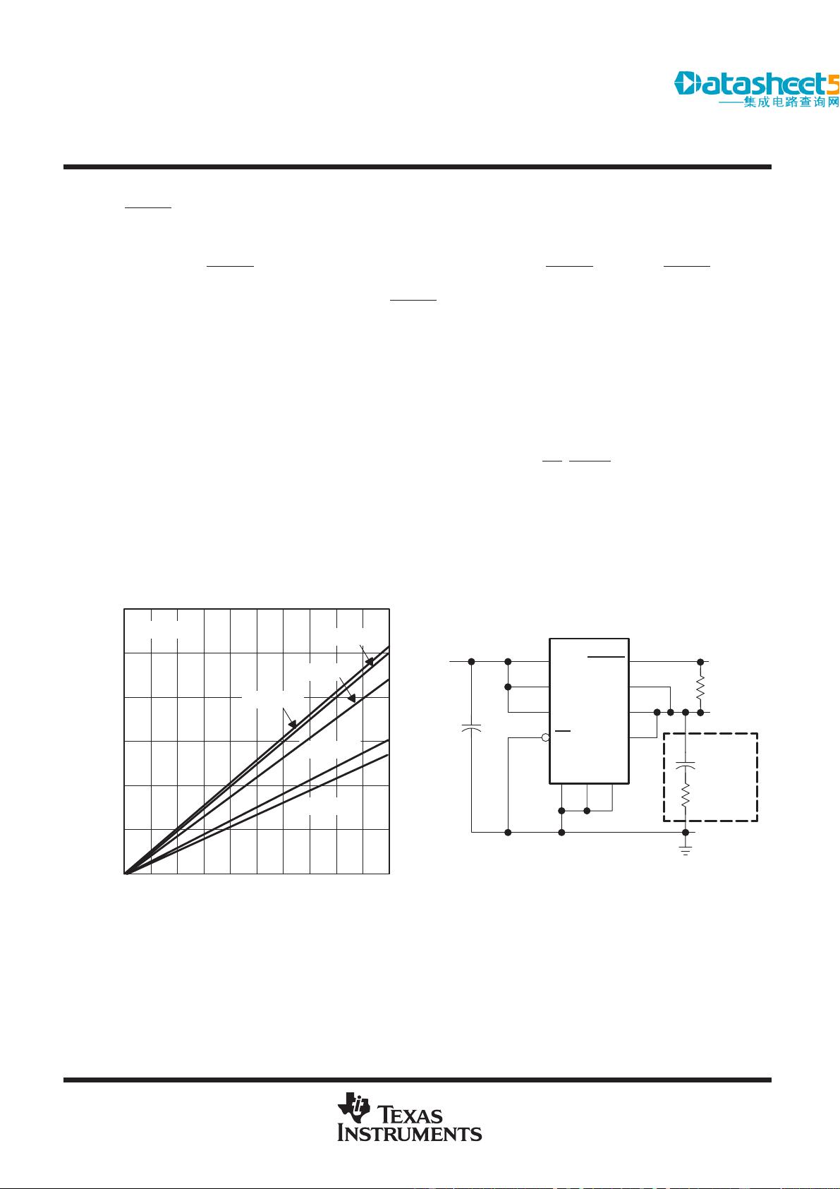
at an output current of 100 mA for the TPS7350) and is directly proportional to the output current (see Figure 1).
Additionally, since the PMOS pass element is a voltage-driven device, the quiescent current is low and remains
constant, independent of output loading (typically 340 µA over the full range of output current, 0 mA to 500 mA).
These two key specifications yield a significant improvement in operating life for battery-powered systems.
The LDO family also features a sleep mode; applying a logic high signal to EN (enable) shuts down the regulator,
reducing the quiescent current to 0.5 µA maximum at T
J
= 25°C.
The TPS73xx is offered in 2.5-V, 3-V, 3.3-V, 4.85-V, and 5-V fixed-voltage versions and in an adjustable version
(programmable over the range of 1.2 V to 9.75 V). Output voltage tolerance is specified as a maximum of 2%
over line, load, and temperature ranges (3% for the 2.5 V and the adjustable version). The TPS73xx family is
available in PDIP (8 pin), SO (8 pin) and TSSOP (20 pin) packages. The TSSOP has a maximum height of
1.2 mm.
Figure 1. Dropout Voltage Versus Output Current
0.25
0.2
0.1
0.05
0
0.15
0 50 100 150 200 250 300
0.3
350 400 450 500
T
A
= 25°C
TPS7348
TPS7350
Dropout Voltage – V
I
O
– Output Current – mA
TPS7333
TPS7330
TPS7325
Figure 2. Typical Application Configuration
†
TPS7325, TPS7330, TPS7333, TPS7348, TPS7350 (fixed-voltage
options)
‡
Capacitor selection is nontrivial. See application information
section for details.
SENSE
RESET
OUT
OUT
9
8
6
10
IN
IN
IN
EN
GND
321
20
15
14
13
V
I
0.1 µF
To System
Reset
CSR = 1 Ω
V
O
10 µF
+
TPS73xxPW
†
C
O
‡
250 kΩ
TPS7301Q, TPS7325Q, TPS7330Q, TPS7333Q, TPS7348Q, TPS7350Q
LOW-DROPOUT VOLTAGE REGULATORS
WITH INTEGRATED DELAYED RESET FUNCTION
SLVS124F – JUNE 1995 – REVISED JANUARY 1999
3
POST OFFICE BOX 655303 • DALLAS, TEXAS 75265
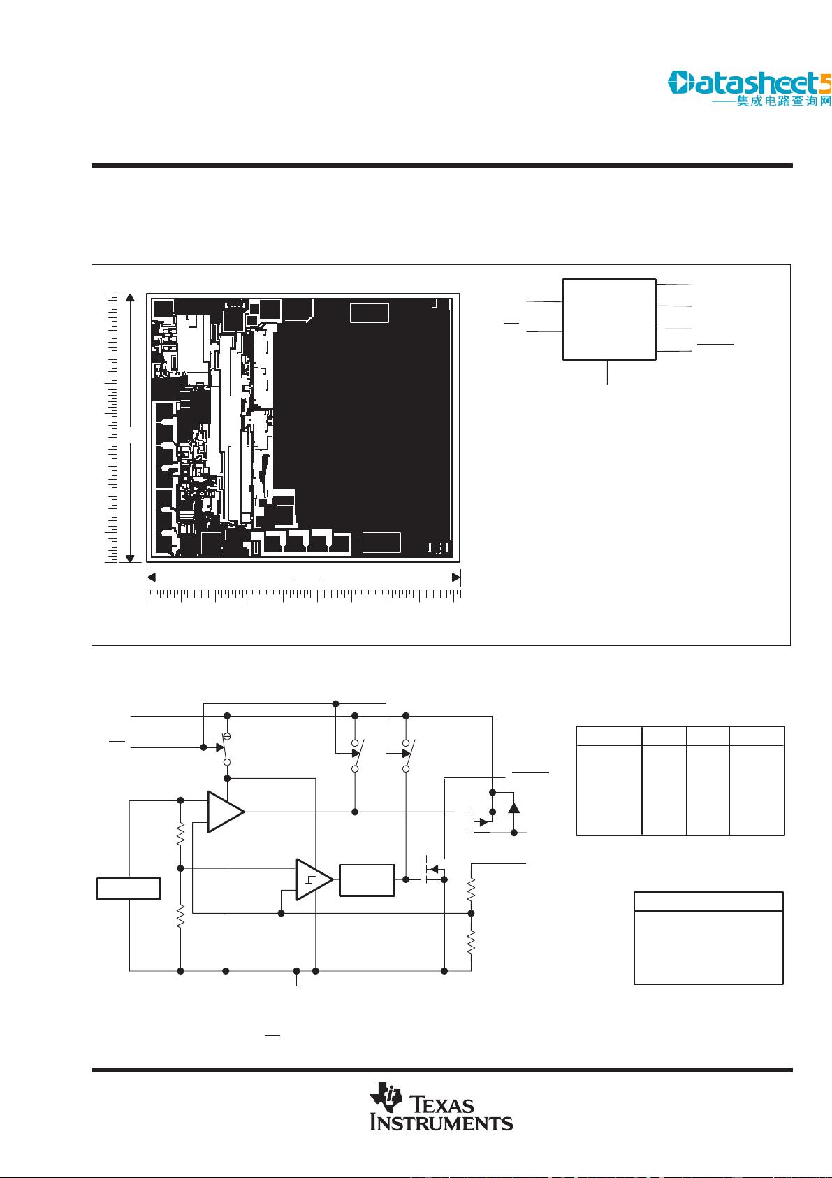
TPS73xxY chip information
These chips, when properly assembled, display characteristics similar to those of the TPS73xxQ. Thermal
compression or ultrasonic bonding may be used on the doped aluminum bonding pads. Chips may be mounted
with conductive epoxy or a gold-silicon preform.
(6)
(4)
(3)
(7)
(2)
(1)
GND
FB
‡
OUT
RESET
IN
EN
TPS73xx
80
92
CHIP THICKNESS: 15 TYPICAL
BONDING PADS: 4 × 4 MINIMUM
T
J
max = 150°C
TOLERANCES ARE ±10%.
ALL DIMENSIONS ARE IN MILS.
†
SENSE – Fixed voltage options only (TPS7325, TPS7330,
TPS7333, TPS7348, and TPS7350)
‡
FB – Adjustable version only (TPS7301)
BONDING PAD ASSIGNMENTS
SENSE
†
(5)
NOTE A. For most applications, OUT and SENSE should
be tied together as close as possible to the device;
for other implementations, refer to SENSE-pin
connection discussion in the applications
information section of this data sheet.
(3)
(4)
(5)
(6)
(7)
(2)
(1)
functional block diagram
¶
_
+
V
ref
OUT
SENSE
§
/FB
EN
IN
GND
R1
R2
RESET
_
+
TPS7301
TPS7325
TPS7330
TPS7333
TPS7348
TPS7350
DEVICE
UNITR1 R2
0
260
358
420
726
756
∞
233
233
233
233
233
Ω
kΩ
kΩ
kΩ
kΩ
kΩ
RESISTOR DIVIDER OPTIONS
§
For most applications, SENSE should be externally connected to OUT as close as possible to the device. For other implementations, refer to
SENSE-pin connection discussion in applications information section.
¶
Switch positions are shown with EN
low (active).
NOTE A. Resistors are nominal values only.
Delayed
Reset
¶¶
MOS transistors
Bilpolar transistors
Diodes
Capacitors
Resistors
COMPONENT COUNT
464
41
4
17
76
TPS7301Q, TPS7325Q, TPS7330Q, TPS7333Q, TPS7348Q, TPS7350Q
LOW-DROPOUT VOLTAGE REGULATORS
WITH INTEGRATED DELAYED RESET FUNCTION
SLVS124F – JUNE 1995 – REVISED JANUARY 1999
4
POST OFFICE BOX 655303 • DALLAS, TEXAS 75265
timing diagram
†
V
res
is the minimum input voltage for a valid RESET. The symbol V
res
is not currently listed within EIA or JEDEC standards
for semiconductor symbology.
ÎÎ
ÎÎ
ÎÎ
ÎÎ
ÎÎ
ÎÎ
ÎÎ
ÎÎ
ÎÎ
ÎÎ
V
I
V
res
†
V
res
t
t
t
V
O
Threshold
Voltage
RESET
Output
200 ms
Delay
200 ms
Delay
Output
Undefined
Output
Undefined
V
IT+
V
IT–
V
IT–
V
IT+
absolute maximum ratings over operating free-air temperature range (unless otherwise noted)
‡
Input voltage range
§
, V
I
, RESET, SENSE, EN –0.3 V to 11 V. . . . . . . . . . . . . . . . . . . . . . . . . . . . . . . . . . . . . . . .
Output current, I
O
2 A. . . . . . . . . . . . . . . . . . . . . . . . . . . . . . . . . . . . . . . . . . . . . . . . . . . . . . . . . . . . . . . . . . . . . . . . . . .
Continuous total power dissipation See Dissipation Rating Tables 1 and 2. . . . . . . . . . . . . . . . . . . . . . . . . . . . .
Operating virtual junction temperature range, T
J
–55°C to 150°C. . . . . . . . . . . . . . . . . . . . . . . . . . . . . . . . . . . . .
Storage temperature range, T
stg
–65°C to 150°C. . . . . . . . . . . . . . . . . . . . . . . . . . . . . . . . . . . . . . . . . . . . . . . . . . .
Lead temperature 1,6 mm (1/16 inch) from case for 10 seconds 260°C. . . . . . . . . . . . . . . . . . . . . . . . . . . . . . .
‡
Stresses beyond those listed under “absolute maximum ratings” may cause permanent damage to the device. These are stress ratings only, and
functional operation of the device at these or any other conditions beyond those indicated under “recommended operating conditions” is not
implied. Exposure to absolute-maximum-rated conditions for extended periods may affect device reliability.
§
All voltage values are with respect to network terminal ground.
TPS7301Q, TPS7325Q, TPS7330Q, TPS7333Q, TPS7348Q, TPS7350Q
LOW-DROPOUT VOLTAGE REGULATORS
WITH INTEGRATED DELAYED RESET FUNCTION
SLVS124F – JUNE 1995 – REVISED JANUARY 1999
5
POST OFFICE BOX 655303 • DALLAS, TEXAS 75265
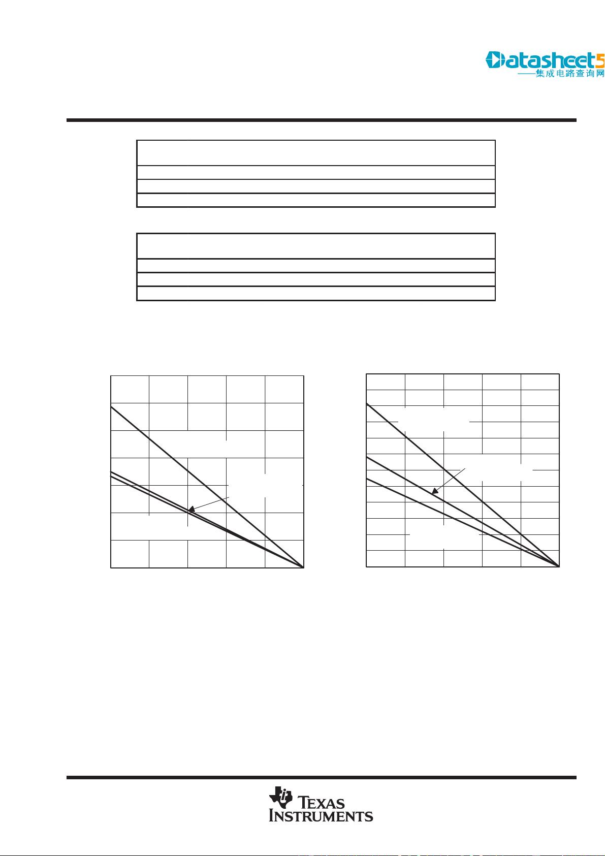
DISSIPATION RATING TABLE 1 – FREE-AIR TEMPERATURE (SEE FIGURE 3)
PACKAGE
T
A
≤ 25°C DERATING FACTOR T
A
= 70°C T
A
= 125°C
PACKAGE
A
POWER RATING ABOVE T
A
= 25°C
A
POWER RATING
A
POWER RATING
D 725 mW 5.8 mW/°C 464 mW 145 mW
P 1175 mW 9.4 mW/°C 752 mW 235 mW
PW
†
700 mW 5.6 mW/°C 448 mW 140 mW
DISSIPATION RATING TABLE 2 – CASE TEMPERATURE (SEE FIGURE 4)
PACKAGE
T
C
≤ 25°C DERATING FACTOR T
C
= 70°C T
C
= 125°C
PACKAGE
C
POWER RATING ABOVE T
C
= 25°C
C
POWER RATING
C
POWER RATING
D 2188 mW 9.4 mW/°C 1765 mW 1248 mW
P 2738 mW 21.9 mW/°C 1752 mW 548 mW
PW
†
4025 mW 32.2 mW/°C 2576 mW 805 mW
†
Refer to Thermal Information section for detailed power dissipation considerations when using the
TSSOP package.
Figure 3
PW Package
R
θJA
= 178°C/W
1200
800
400
0
25 50 75 100
– Maximum Continuous Dissipation – mW
MAXIMUM CONTINUOUS DISSIPATION
vs
FREE-AIR TEMPERATURE
125 150
1400
1000
600
200
P
D
T
A
– Free-Air Temperature – °C
D Package
R
θJA
= 172°C/W
P Package
R
θJA
= 106°C/W
Figure 4
2400
1600
800
0
25 50 75 100
– Maximum Continuous Dissipation – mW
3200
4000
MAXIMUM CONTINUOUS DISSIPATION
vs
CASE TEMPERATURE
4800
125 150
4400
3600
2800
2000
1200
400
P
D
T
C
– Case Temperature – °C
D Package
R
θJC
= 57°C/W
P Package
R
θJC
= 46°C/W
PW Package
R
θJC
= 37°C/W
剩余43页未读,继续阅读
资源评论

wuminghong_xmu
- 粉丝: 0
- 资源: 6
上传资源 快速赚钱
 我的内容管理
展开
 我的资源
快来上传第一个资源
 我的收益 登录查看自己的收益
 我的积分
登录查看自己的积分
 我的C币
登录后查看C币余额
 我的收藏
我的收藏  我的下载
我的下载  下载帮助
下载帮助

 前往需求广场,查看用户热搜
最新资源
- STM32开发 IIR带阻滤波器 STM32实现IIR无限冲击响应带阻滤波器设计,巴特沃斯滤波器,代码工整,自编代码,注释详细,赠送巴特沃斯和切比雪夫IIR带阻滤波器MATLAB程序
- 四轴抓取视觉旋转标定源代码,学习机器视觉和运动控制的最佳例子,基于VS2015 C++ 实现,仿雅马哈四轴机械手抓取程序,实现把两个任意摆放的物料通过视觉算法和运动控制指令定位摆放到指定的位置并拼接起
- COOFDM的Matlab仿真程序,包括文档代码解释和理论解释
- 伺服驱动器,你还在为伺服驱动器 FPGA架构苦恼吗,本方案FPGA代码实现电流环 速度环 位置环 SVPWM 坐标变 测速 分频 滤波器等,程序方便移植不同的平台,具有很高的研究价值
- omron欧姆龙CJ CP程序 欧姆龙CJ2M-CPU35,主机架搭载两套从机架,ID263.OD263等输入输出IO模块 全自动电池注液封装机,NC413四轴模块轴控制,SCU31无协议读写欧姆龙E
- 基于PI控制器的单相逆变器闭环控制模型,采用电压电流双环控制 波形输出良好,输出跟随给定220V交流输出 运行环境为matlab simulink plecs等
- PLC案例 污水处理系统 - 污水处理项目 某大厂技术给某国企做的污水处理项目,程序规范,图纸清晰,具有很好的参考价值 PLC: 西门子s7 200smart 系统涉及好氧发酵、厌氧发酵、冷热水P
资源上传下载、课程学习等过程中有任何疑问或建议,欢迎提出宝贵意见哦~我们会及时处理!
点击此处反馈


安全验证
文档复制为VIP权益,开通VIP直接复制
 信息提交成功