


ADV7611 Reference Manual
UG-180
One Technology Way • P. O. Box 9106 • Norwood, MA 02062-9106, U.S.A. • Te l: 781.329.4700 • Fax: 781.461.3113 • www.analog.com
Advantiv ADV7611 HDMI Receiver Functionality and Features
PLEASE SEE THE LAST PAGE FOR AN IMPORTANT
WARNING AND LEGAL TERMS AND CONDITIONS.
Rev. D | Page 1 of 184
SCOPE
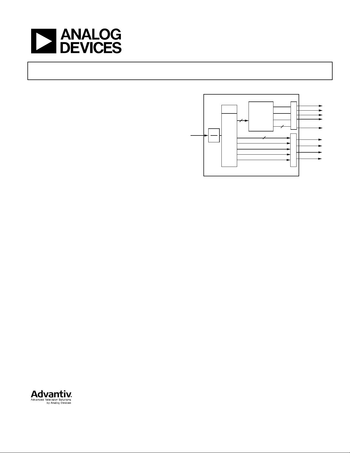
This user guide provides a detailed description of the Advantiv™ ADV7611 HDMI® receiver functionality and features.
DISCLAIMER
Information furnished by Analog Devices, Inc., is believed to be accurate and reliable. However, no responsibility is assumed by Analog
Devices for its use, nor any infringements of patents or other rights of third parties that may result from its use.
Specifications are subject to change without notice. No license is granted by implication or otherwise under any patent or patent rights of
Analog Devices. Trademarks and registered trademarks are the property of their respective owners.
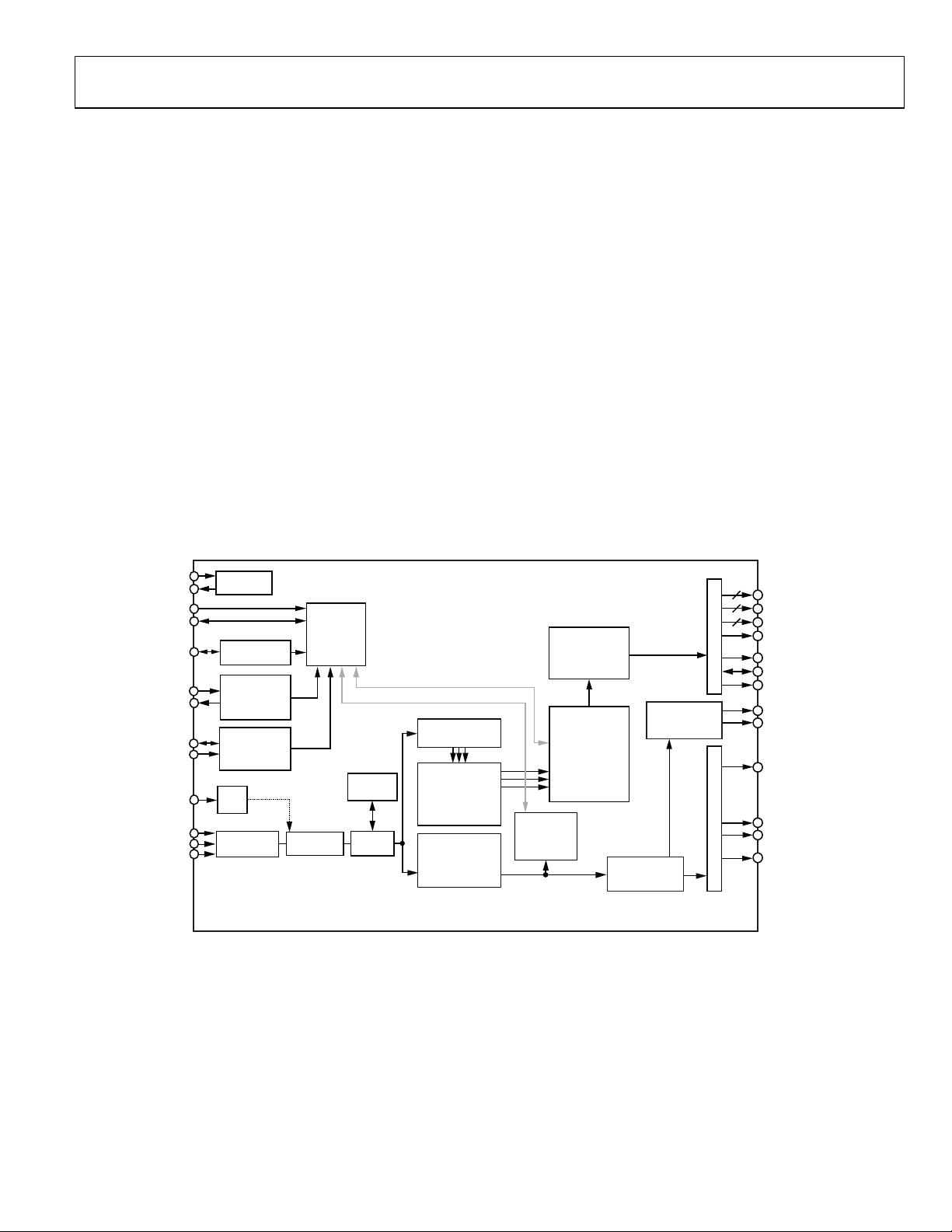
FUNCTIONAL BLOCK DIAGRAM
ADV7611
09238-001
DPLL
CEC
CONTROLLER
5V DETECT
AND HPD
CONTROLLER
CONTROL
INTERFACE
I
2
C
XTALP
P0 TO P7
P8 TO P15
AP
P16 TO P23
LLC
LRCLK
SCLK/INT2*
MCLK/INT2*
HS
VS/FIELD/ALSB
DE
INT1
INT2*
XTALN
RXA_5V
HPA_A/INT2*
EDID
REPEATER
CONTROLLER
PLL
EQUALIZER EQUALIZER
HDCP
ENGINE
HDCP
EEPROM
DATA
PREPROCESSOR
AND COLOR
SPACE
CONVERSION
COMPONENT
PROCESSOR
BACKEND
COLOR SPACE
CONVERSION
PACKET
PROCESSOR
PACKET/
INFOFRAME
MEMORY
HDMI
PROCESSOR
DDCA_SDA
DDCA_SCL
RXA_0±
RXA_2±
RXA_1±
SCL
SDA
CEC
RXA_C±
CONTROL
AND DATA
A
B
C
AUDIO OUTPUT FORMATTER OUTPUT FORMATTER
INTERRUPT
CONTROLLER
(INT1, INT2)
*INT2 CAN BE ONLY OUTPUT ON ONE OF THE PINS: SCLK/INT2, MCLK/INT2, OR HPA_A/INT2.
AUDIO
PROCESSOR
MUTE
12
12
12
Figure 1.

UG-180 ADV7611 Reference Manual
Rev. D | Page 2 of 184
TABLE OF CONTENTS
Scope .................................................................................................. 1
Disclaimer .......................................................................................... 1
Functional Block Diagram .............................................................. 1
Revision History ............................................................................... 5
Using the ADV7611 Hardware User Guide .................................. 6
Number Notations ........................................................................ 6
Register Access Conventions ...................................................... 6
Acronyms and Abbreviations ..................................................... 6
Field Function Descriptions ........................................................ 8
Example Field Function Description ..................................... 8
References ...................................................................................... 8
Introduction to the ADV7611 ........................................................ 9
HDMI Receiver ............................................................................. 9
Component Processor ................................................................. 9
Main Features of ADV7611 ........................................................ 9
HDMI Receiver ......................................................................... 9
Component Video Processing ................................................ 9
Video Output Formats ........................................................... 10
Additional Features ................................................................ 10
Pin Configuration and Function Descriptions ....................... 11
Global Control Registers ............................................................... 13
ADV7611 Revision Identification ............................................ 13
Power-Down Controls ............................................................... 13
Primary Power-Down Controls ........................................... 13
Secondary Power-Down Controls ....................................... 13
Power-Down Modes .............................................................. 14
Global Pin Control ..................................................................... 15
Reset Pin .................................................................................. 15
Reset Controls ......................................................................... 15
Tristate Output Drivers ......................................................... 15
Tristate LLC Driver ................................................................ 16
Tristate Synchronization Output Drivers ............................ 16
Tristate Audio Output Drivers.............................................. 16
Drive Strength Selection ........................................................ 17
Output Synchronization Selection ....................................... 17
Output Synchronization Signals Polarity ............................ 18
Digital Synthesizer Controls ................................................. 19
Crystal Frequency Selection ................................................. 19
Primary Mode and Video Standard ............................................. 20
Primary Mode and Video Standard Controls ......................... 20
V_FREQ .................................................................................. 22
HDMI Decimation Modes ........................................................ 22
Primary Mode and Video Standard Configuration for HDMI
Free Run ....................................................................................... 23
Recommended Settings for HDMI Inputs .............................. 23
Pixel Port Configuration ............................................................... 25
Pixel Port Output Modes ........................................................... 25
Bus Rotation and Reordering Controls ............................... 25
Pixel Data and Synchronization Signals Control ............... 25
LLC Controls............................................................................... 26
DLL on LLC Clock Path ............................................................ 26
Adjusting DLL Phase in All Modes ..................................... 26
DLL Settings for 656, 8-/10-/12-Bit Modes ........................ 27
HDMI Receiver ............................................................................... 28
+5 V Cable Detect ...................................................................... 28
Hot Plug Assert ........................................................................... 29
E-EDID/Repeater Controller .................................................... 31
E-EDID Data Configuration..................................................... 31
Notes ........................................................................................ 32
E-EDID Support for Power-Down Modes ......................... 32
Transitioning of Power Modes ................................................. 32
Structure of Internal E-EDID ................................................... 32
Notes ........................................................................................ 33
TMDS Equalization ................................................................... 33
Port Selection .............................................................................. 33
TMDS Clock Activity Detection .............................................. 33
Important ................................................................................ 34
Clock and Data Termination Control ................................. 34
HDMI/DVI Status Bits .............................................................. 34
Video 3D Detection ................................................................... 34
TMDS Measurement.................................................................. 35
TMDS Measurement after TMDS PLL ............................... 35
Deep Color Mode Support ........................................................ 36
Notes ........................................................................................ 36
Video FIFO .................................................................................. 36
Pixel Repetition .......................................................................... 38
HDCP Support ........................................................................... 39
HDCP Decryption Engine .................................................... 39
Internal HDCP Key OTP ROM ........................................... 40
HDCP Keys Access Flags ...................................................... 40
ADV7611 Reference Manual UG-180
Rev. D | Page 3 of 184
HDCP Ri Expired ................................................................... 41
HDMI Synchronization Parameters ......................................... 42
Notes ......................................................................................... 42
Horizontal Filter and Measurements ................................... 42
Primary Port Horizontal Filter Measurements ................... 42
Horizontal Filter Locking Mechanism ................................. 44
Vertical Filters and Measurements ....................................... 44
Primary Port Vertical Filter Measurements ........................ 44
Vertical Filter Locking Mechanism ...................................... 47
Low Frequency Formats ......................................................... 47
Audio Control and Configuration ............................................ 47
Important ................................................................................. 48
Audio DPLL ............................................................................. 48
Locking Mechanism ............................................................... 48
ACR Parameters Loading Method ....................................... 48
Audio DPLL Coast Feature .................................................... 48
Audio FIFO .................................................................................. 49
Audio Packet Type Flags ............................................................ 50
Notes ......................................................................................... 51
Audio Output Interface .............................................................. 52
I
2
S/SPDIF Audio Interface and Output Controls ............... 53
Notes ......................................................................................... 54
MCLKOUT Setting ..................................................................... 56
Audio Channel Mode ................................................................. 56
Audio Muting .............................................................................. 57
Delay Line Control ................................................................. 57
Audio Mute Configuration .................................................... 57
Internal Mute Status ............................................................... 60
AV Mute Status ........................................................................ 60
Audio Mute Signal .................................................................. 60
Audio Stream with Incorrect Parity Error ........................... 61
Audio Clock Regeneration Parameters .................................... 61
ACR Parameters Readbacks .................................................. 61
Monitoring ACR Parameters ................................................. 61
Channel Status ............................................................................. 62
Validity Status Flag .................................................................. 62
General Control and Mode Information ............................. 63
Category Code ......................................................................... 64
Source Number and Channel Number ................................ 64
Sampling and Frequency Accuracy ...................................... 65
Word Le ngth ............................................................................ 65
Channel Status Copyright Value Assertion ......................... 66
Monitoring Change of Audio Sampling Frequency ........... 66
Packets and InfoFrames Registers ............................................ 66
InfoFrames Registers .............................................................. 66
InfoFrame Collection Mode .................................................. 67
InfoFrame Checksum Error Flags ........................................ 67
AVI InfoFrame Registers ....................................................... 68
Audio InfoFrame Registers .................................................... 69
SPD InfoFrame Registers ....................................................... 70
MPEG Source InfoFrame Registers ...................................... 71
Vendor Specific InfoFrame Registers ................................... 72
Packet Registers ........................................................................... 73
ACP Packet Registers ............................................................. 73
ISRC Packet Registers............................................................. 74
Gamut Metadata Packets ....................................................... 76
Customizing Packet/InfoFrame Storage Registers ................. 77
Repeater Support ......................................................................... 78
Repeater Routines Performed by the EDID/Repeater
Controller ................................................................................. 78
Repeater Actions Required by External Controller ........... 79
HDCP Registers Available in Repeater Map ....................... 80
Interface to DPP Section ............................................................ 85
Notes ......................................................................................... 86
Pass Through Mode .................................................................... 86
4:2:2 Pass Through .................................................................. 86
4:4:4 Pass Through .................................................................. 86
Color Space Information Sent to the DPP and CP Sections . 87
Status Registers ............................................................................ 87
HDMI Section Reset Strategy ................................................... 90
HDMI Packet Detection Flag Reset.......................................... 90
Data Preprocessor and Color Space Conversion and Color
Controls ............................................................................................ 91
Color Space Conversion Matrix ................................................ 91
CP CSC Selection .................................................................... 91
Selecting Auto or Manual CP CSC Conversion Mode ...... 92
Auto Color Space Conversion Matrix .................................. 92
HDMI Automatic CSC Operation........................................ 94
Manual Color Space Conversion Matrix ............................. 96
CSC in Pass-Through Mode ................................................ 100
Color Controls ........................................................................... 100
Component Processor .................................................................. 102
Introduction to the Component Processor ........................... 102

UG-180 ADV7611 Reference Manual
Rev. D | Page 4 of 184
Clamp Operation ...................................................................... 102
CP Gain Operation................................................................... 104
Features of Manual Gain Control ...................................... 104
Features of Automatic Gain Control ................................. 104
Manual Gain and Automatic Gain Control Selection ..... 104
Manual Gain Control ........................................................... 105
Manual Gain Filter Mode .................................................... 107
Other Gain Controls ............................................................ 107
CP Offset Block......................................................................... 108
Notes ...................................................................................... 108
AV Code Block .......................................................................... 109
CP Data Path for HDMI Modes ............................................. 111
Pregain Block ........................................................................ 111
Sync Processed by CP Section ................................................ 114
Sync Routing from HDMI Section .................................... 114
Standard Detection and Identification .............................. 114
Detailed Mechanism of STDI Block Horizontal/Vertical
Lock Mechanism .................................................................. 117
CP Output Synchronization Signal Positioning ................... 121
CP Synchronization Signals ................................................ 123
HSync Timing Controls ...................................................... 123
VSync Timing Controls ....................................................... 125
DE Timing Controls ............................................................ 127
FIELD Timing Controls ...................................................... 128
HCOUNT Timing Control ................................................. 132
CP HDMI Controls .................................................................. 133
Free Run Mode ......................................................................... 133
Free Run Mode Thresholds ................................................. 133
Free Run Feature in HDMI Mode ...................................... 135
Free Run Default Color Output .......................................... 136
CP Status .................................................................................... 137
CP_REG_FF .......................................................................... 137
CP Core Bypassing ................................................................... 137
Consumer Electronics Control ................................................... 138
Main Controls ........................................................................... 138
CEC Transmit Section ............................................................. 139
CEC Receive Section ................................................................ 141
Logical Address Configuration .......................................... 141
Receive Buffers ...................................................................... 142
CEC Message Reception Overview .................................... 145
Antiglitch Filter Module .......................................................... 146
Typical Operation Flow ........................................................... 147
Initializing CEC Module ..................................................... 147
Using CEC Module as Initiator .......................................... 148
Using CEC Module as Follower ......................................... 149
Low Power CEC Message Monitoring ................................... 150
Interrupts ....................................................................................... 152
Interrupt Architecture Overview ........................................... 152
Interrupt Pins ............................................................................ 155
Notes ...................................................................................... 155
Interrupt Duration ............................................................... 156
Interrupt Drive Level ........................................................... 156
Interrupt Manual Assertion ................................................ 156
Multiple Interrupt Events .................................................... 157
Description of Interrupt Bits .................................................. 158
General Operation ............................................................... 158
HDMI Video Mode .............................................................. 158
CEC ........................................................................................ 158
HDMI Only Mode ............................................................... 158
Additional Explanations .......................................................... 159
STDI_DATA_VALID_RAW ............................................... 159
CP_LOCK, CP_UNLOCK ................................................. 160
HDMI Interrupts Validity Checking Process ................... 160
Storing Masked Interrupts .................................................. 162
Register Access and Serial Ports Description ........................... 173
Main I
2
C Port ............................................................................ 173
Register Access ..................................................................... 173
IO I
2
C Map Address ............................................................. 173
Addresses of Other Maps .................................................... 174
Protocol for Main I
2
C Port .................................................. 175
DDC Ports ................................................................................. 176
I
2
C Protocols for Access to the Internal EDID ................. 176
I
2
C Protocols for Access to HDCP Registers .................... 176
DDC Port A .......................................................................... 176
Appendix A ................................................................................... 177
PCB Layout Recommendations ............................................. 177
Power Supply Bypassing .......................................................... 177
Example of a Current Loop................................................. 177
Digital Outputs (Data and Clocks) ........................................ 177
Digital Inputs ............................................................................ 178
XTAL and Load Cap Value Selection .................................... 178
Example ................................................................................. 178

ADV7611 Reference Manual UG-180
Rev. D | Page 5 of 184
Appendix B .................................................................................... 179
Recommended Unused Pin Configurations ........................ 179
Appendix C ................................................................................... 181
Pixel Output Formats ............................................................... 181
REVISION HISTORY
5
/2017—Rev. C to Rev. D
Cha
nges to Audio Muting Section ................................................ 57
2/2014—Re
v. B to Rev. C
Changes to DDC_PWRDN, Addr 68 (HDMI),
Address 0x73[0] Section ................................................................. 15
Changes to Code 0110; Table 6...................................................... 21
Changes to HDMI_PORT_SELECT[2:0], Addr 68 (HDMI),
Address 0x00[2:0] Section .............................................................. 33
Changes to Video 3D Detection Section ...................................... 34
11/2012
—Rev. A to Rev. B
Deleted TDM from Table 3 .............................................................. 7
Deleted TDM Information from Introduction to the
ADV7611 Section .............................................................................. 9
Changes to Pin 1 and Pin 48 Descriptions ................................... 11
Changes to ADV7611 Revision Identification Section .............. 13
Changes to Table 5 .......................................................................... 14
Changes to INV_F_POL, IO, Address 0x06[3] Section ............. 18
Changes to DLL Settings for 656, 8-/10-/12-Bit Modes Section
and Added Table 9 ........................................................................... 27
Changes to E-EDID Data Configuration Section ....................... 31
Changes to Figure 4......................................................................... 33
Changes to HDMI/DVI Status Bits Section ................................. 34
Added Low Frequency Formats Section and Figure 12 and
Changes to Audio Control and Configuration Section ............. 47
Changes to Table 12 ........................................................................ 52
Deleted I2S_TDM_MODE_ENABLE, Addr 68 (HDMI),
Address 0x6D[7] Section ................................................................ 53
Changes to Notes Section ............................................................... 54
Deleted Figure 20 and Changes to MCLK_FS_N[2:0], Addr 4C
(DPLL), Address 0xB5[2:0] Section .............................................. 56
Changes to Audio Mute Signal Section ........................................ 60
Changes to XTAL and Load Cap Value Selection Section .......178
Changes to Table 73 ......................................................................181
Changes to Ta
ble 74 ......................................................................182
12/2011—Rev. 0 to Rev. A
Change to Video Output Formats Section ................................... 10
Changes to RD_INFO[15:0] Table in ADV7611 Revision
Identification Section ..................................................................... 13
Change to XTAL_FREQ_SEL[1:0] Table in Crystal
Frequency Selection Section .......................................................... 19
Changes to Table 7 .......................................................................... 23
Added Endnote to OP_FORMAT_SEL[7:0] Table in Pixel
Port Output Modes Section ........................................................... 25
Added LLC_DLL_DOUBLE to DLL on LLC Clock Path
Section .............................................................................................. 26
Added DLL Settings for 656, 8-/10-/12-Bit Modes Section ...... 27
Changes to Audio Mute Signal Section ........................................ 61
Added 1001 to CS_DATA[27:24] Table in Sampling and
Frequency Accuracy Section ......................................................... 66
Changes to Check the Value of Each Coefficient Section ....... 100
Changes to CP_HUE[7:0], Addr 44 (CP), Address 0x3D[7:0]
in Color Controls Section; Changes to CP_HUE[7:0] Table ..... 102
Changes to INT2_POL Table in Interrupt Drive Level Section ... 157
Added Endnote to Table 71 ......................................................... 182
10/2010—Revision 0: Initial Version


评论0