GS2971A芯片手册
需积分: 50 75 浏览量
2021-07-23
16:56:07
上传
评论 1
收藏 4.52MB PDF 举报

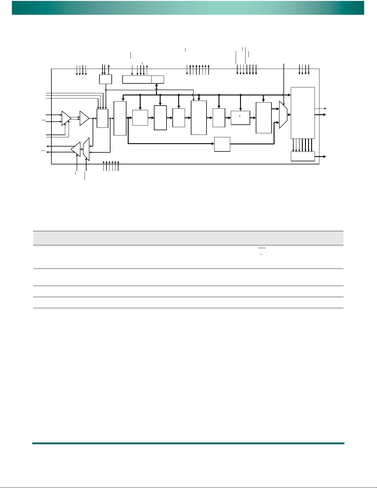
1 of 150GS2971A 3Gb/s, HD, SD SDI Receiver
Final Data Sheet Rev. 3
GENDOC-054311 July 2013
3Gb/s, HD, SD SDI Receiver, with Integrated Adaptive Cable Equalizer complete
with SMPTE Audio and Video Processing
GS2971A
www.semtech.com
Key Features
• Operation at 2.97Gb/s, 2.97/1.001Gb/s, 1.485Gb/s,
1.485/1.001Gb/s and 270Mb/s
• Supports SMPTE ST 425 (Level A and Level B),
SMPTE ST 424, SMPTE ST 292, SMPTE ST 259-C and
DVB-ASI
• Integrated adaptive cable equalizer
• Typical equalized length of Belden 1694A cable:
150m at 2.97Gb/s
250m at 1.485Gb/s
480m at 270Mb/s
• Integrated Reclocker with low phase noise, integrated
VCO
• Serial digital reclocked, or non-reclocked output
• Integrated audio de-embedder for 8 channels of 48kHz
audio
• Integrated audio clock generator
• Ancillary data extraction
• Optional conversion from SMPTE ST 425 Level B to
Level A for 1080p 50/60 4:2:2 10-bit
• Parallel data bus selectable as either 20-bit or 10-bit
• Comprehensive error detection and correction
features
• Output H, V, F or CEA 861 Timing Signals
• 1.2V digital core power supply, 1.2V and 3.3V analog
power supplies, and selectable 1.8V or 3.3V I/O power
supply
• GSPI Host Interface
• -20ºC to +85ºC operating temperature range
• Low power operation (typically 545mW)
• Small 11mm x 11mm 100-ball BGA package
• Pb-free and RoHS compliant
Applications
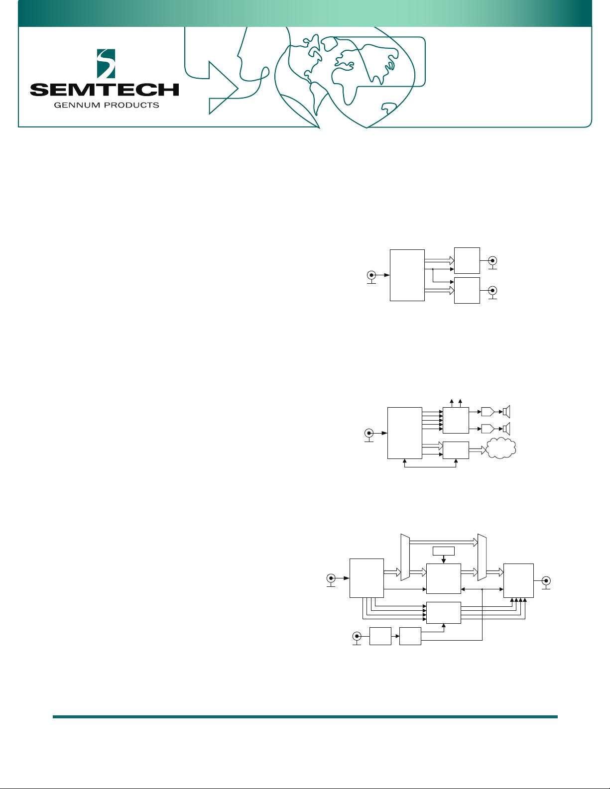
HD-SDI
Application: Single Link (3G-SDI)
to Dual Link (HD-SDI) Converter
GS2962/72
Link A
Link B
HV F/PCLK
10-bit
3G-SDI
GS2971A
GS2962/72
10-bit
HV F/PCLK
HD-SDI
Application: 1080p50/60 Monitor
Audio
Selector
Video
Processor
10-bit
HV F/PCLK
CTR L/TIMECODE
AES - OUT
AUDIO 1/2
Audio C locks
Speakers
Display
DAC
DAC
3G-SDI
GS2971A
AUDIO 3/4
AUDIO 5/6
AUDIO 7/8
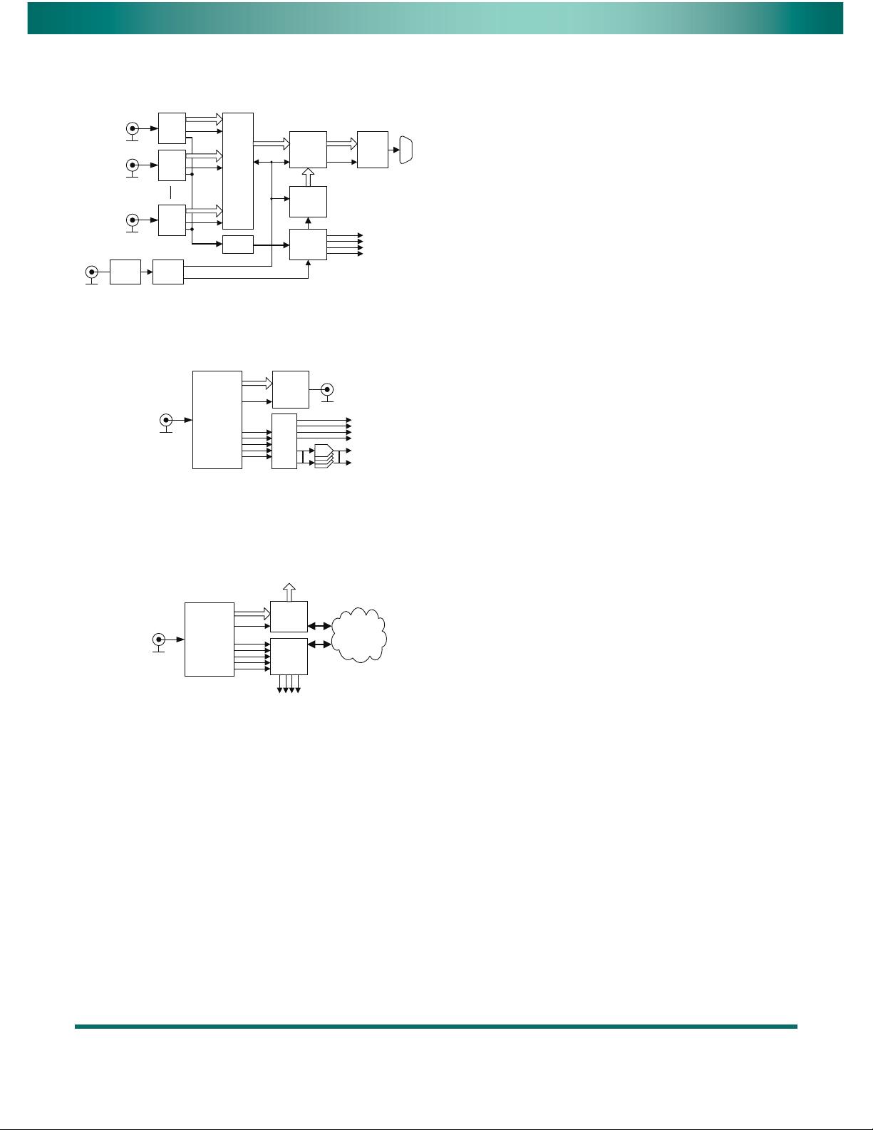
Application: Multi-format Downconverter
Audio
Processing
& Delay
GS4901
Analog
Sync
Sync
Seperator
10-bit
HV F/PCLK
HD/SD
Serializer
(GS1582,
GS1672)
Video
Downconver ter &
Aspect Ratio
Conversion
Memory
10-bit
10-bit bit SD Bypass
HV F/PCLK
Audio Clocks
AE S 1/2
AE S 3/4
AE S 5/6
AE S 7/8
SD-SDI
SD/HD/3G-SDI
GS2971A
AE S 1/2
AE S 3/4
AE S 5/6
AE S 7/8


剩余149页未读,继续阅读
资源评论


