没有合适的资源?快使用搜索试试~ 我知道了~
TI-TS3L100.pdf
0 下载量 120 浏览量
2022-12-16
21:46:23
上传
评论 3
收藏 1.51MB PDF 举报
温馨提示
试读
30页
以太网开关
资源推荐
资源详情
资源评论
SCDS161A − MAY 2004 – REVISED OCTOBER 2004
1
POST OFFICE BOX 655303 • DALLAS, TEXAS 75265
D Wide Bandwidth (BW = 350 MHz Min)
D Low Differential Crosstalk
(X
TALK
= −68 dB Typ)
D Low Power Consumption (I
CC
= 10 mA Max)
D Bidirectional Data Flow, With Near-Zero
Propagation Delay
D Low ON-State Resistance (r
on
= 5 W Typ)
D Rail-to-Rail Switching on Data I/O Ports
(0 to V
CC
)
D V
CC
Operating Range From 3 V to 3.6 V
D I
off
Supports Partial-Power-Down Mode
Operation
D Data and Control Inputs Have Undershoot
Clamp Diodes
D Latch-Up Performance Exceeds 100 mA Per
JESD 78, Class II
D ESD Performance Tested Per JESD 22
− 2000-V Human-Body Model
(A114-B, Class II)
− 1000-V Charged-Device Model (C101)
D Suitable for Both 10 Base-T/100 Base-T
Signaling
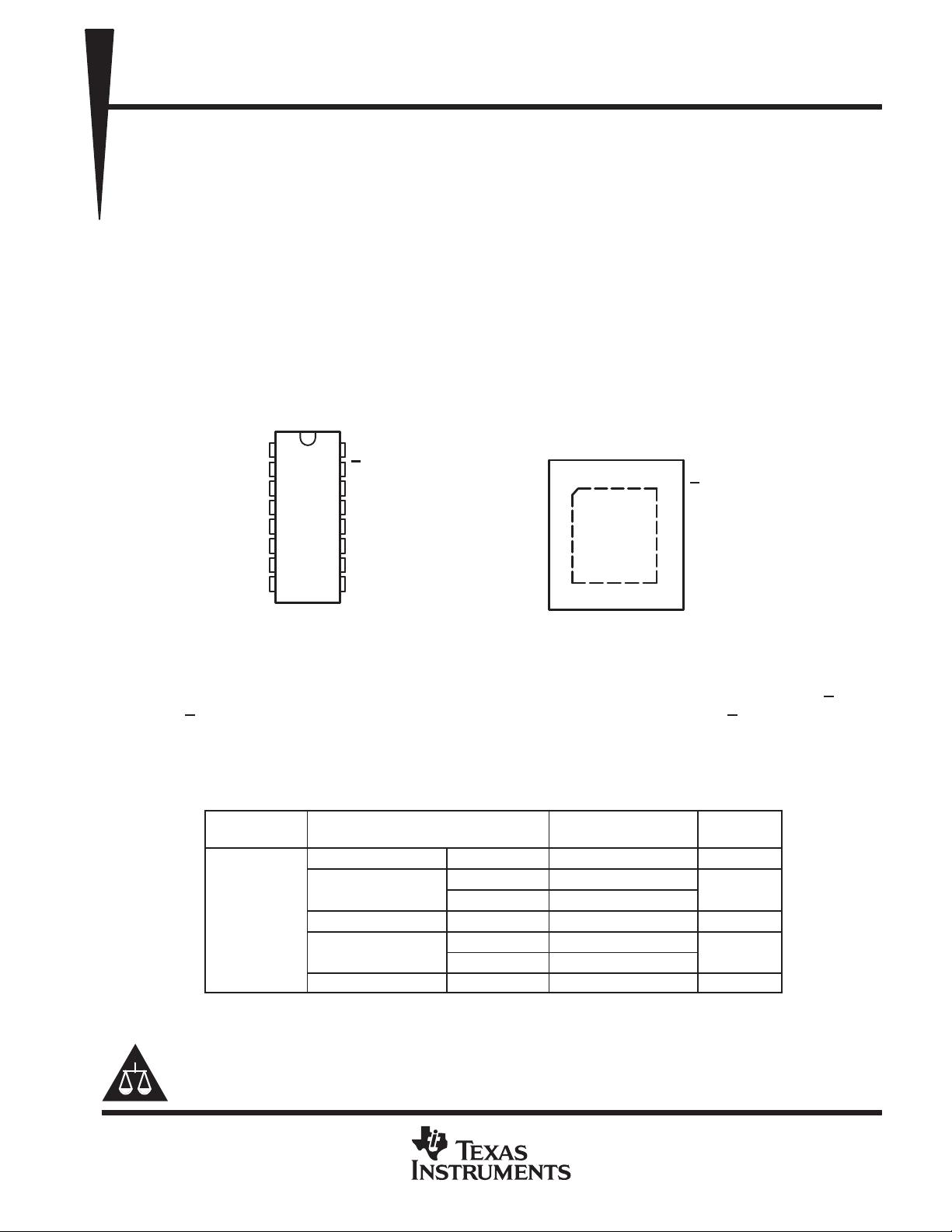
D, DBQ, DGV, OR PW PACKAGE
(TOP VIEW)
1
2
3
4
5
6
7
8
16
15
14
13
12
11
10
9
S
IA
0
IA
1
YA
IB
0
IB
1
YB
GND
V
CC
E
ID
0
ID
1
YD
IC
0
IC
1
YC
RGY PACKAGE
(TOP VIEW)
116
89
2
3
4
5
6
7
15
14
13
12
11
10
E
ID
0
ID
1
YD
IC
0
IC
1
IA
0
IA
1
YA
IB
0
IB
1
YB
S
YC
V
GND
CC
description/ordering information
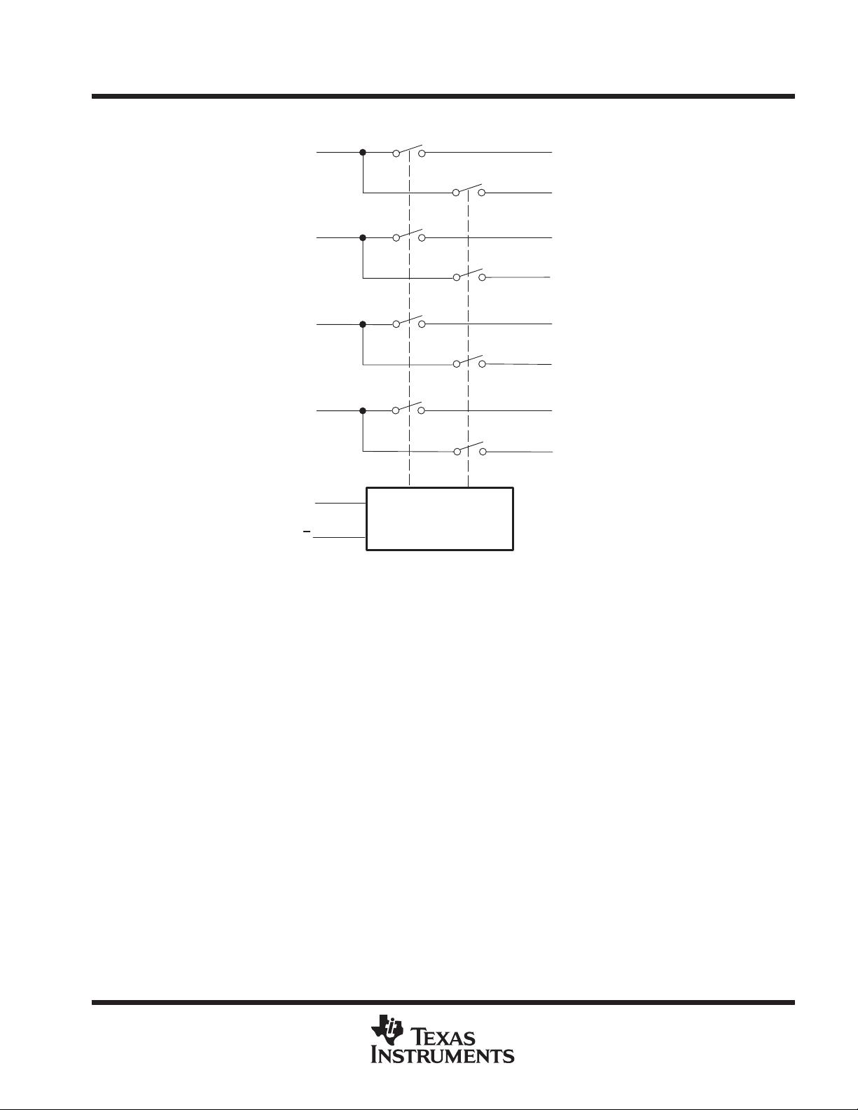
The TI TS3L100 LAN switch is a 4-bit 1-of-2 multiplexer/demultiplexer with a single switch-enable (E) input.
When E
is low, the switch is enabled and the I port is connected to the Y port. When E is high, the switch is
disabled and the high-impedance state exists between the I and Y ports. The select (S) input controls the data
path of the multiplexer/demultiplexer.
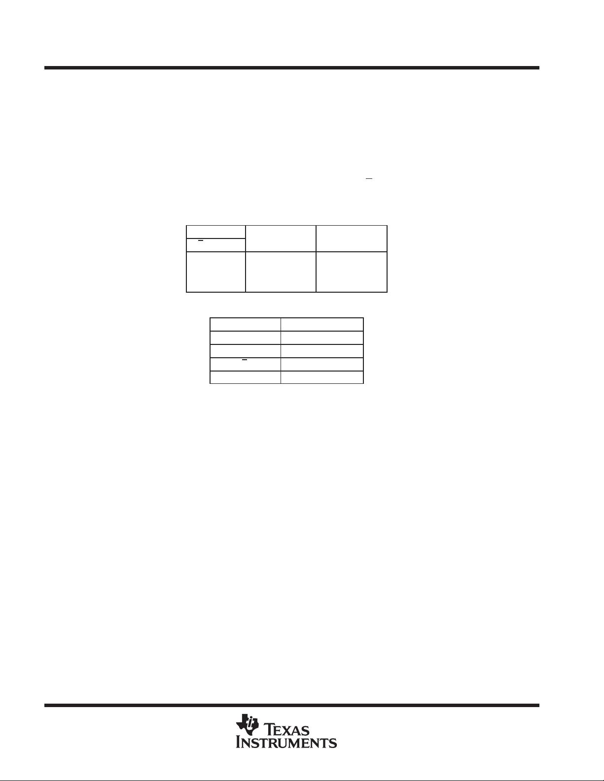
ORDERING INFORMATION
T
A
PACKAGE
†
ORDERABLE
PART NUMBER
TOP-SIDE
MARKING
QFN − RGY Tape and reel TS3L100RGYR TK100
SOIC − D
Tube TS3L100D
TS3L100
SOIC − D
Tape and reel TS3L100DR
TS3L100
0°C to 70°C
SSOP (QSOP) − DBQ Tape and reel TS3L100DBQR TK100
0 C to 70 C
TSSOP − PW
Tube TS3L100PW
TK100
TSSOP − PW
Tape and reel TS3L100PWR
TK100
TVSOP − DGV Tape and reel TS3L100DGVR TK100
†
Package drawings, standard packing quantities, thermal data, symbolization, and PCB design guidelines
are available at www.ti.com/sc/package.
Copyright 2004, Texas Instruments Incorporated
Please be aware that an important notice concerning availability, standard warranty, and use in critical applications of
Texas Instruments semiconductor products and disclaimers thereto appears at the end of this data sheet.
!" #!$% &"'
&! #" #" (" " ") !"
&& *+' &! #", &" ""%+ %!&"
", %% #""'
SCDS161A − MAY 2004 – REVISED OCTOBER 2004
2
POST OFFICE BOX 655303 • DALLAS, TEXAS 75265
description/ordering information (continued)
This device can be used to replace mechanical relays in LAN applications. This device has low r
on
, wide
bandwidth, and low differential crosstalk, making it suitable for 10 Base-T, 100 Base-T, and various other LAN
applications.
This device is fully specified for partial-power-down applications using I
off
. The I
off
feature ensures that
damaging current will not backflow through the device when it is powered down. The device has isolation during
power off.
To ensure the high-impedance state during power up or power down, E
should be tied to V
CC
through a pullup
resistor; the minimum value of the resistor is determined by the current-sinking capability of the driver.
FUNCTION TABLE
INPUTS
INPUT/OUTPUT
FUNCTION
E S
INPUT/OUTPUT
YX
FUNCTION
L L IX
0
YX = IX
0
L HIX
1
YX = IX
1
H X Z Disconnect
PIN DESCRIPTIONS
PIN NAME
DESCRIPTION
IAn−IDn Data I/Os
S Select input
E Enable input
YA−YD Data I/Os
SCDS161A − MAY 2004 – REVISED OCTOBER 2004
3
POST OFFICE BOX 655303 • DALLAS, TEXAS 75265
logic diagram (positive logic)
YA
IA
0
IA
1
IB
0
IB
1
IC
0
IC
1
ID
0
ID
1
E
S
YC
YB
YD
4
7
9
12
2
3
5
6
11
10
14
13
15
1
Control
Logic
SCDS161A − MAY 2004 – REVISED OCTOBER 2004
4
POST OFFICE BOX 655303 • DALLAS, TEXAS 75265
absolute maximum ratings over operating free-air temperature range (unless otherwise noted)
†
Supply voltage range, V
CC
−0.5 V to 4.6 V. . . . . . . . . . . . . . . . . . . . . . . . . . . . . . . . . . . . . . . . . . . . . . . . . . . . . . . . .
Control input voltage range, V
IN
(see Notes 1 and 2) −0.5 V to 4.6 V. . . . . . . . . . . . . . . . . . . . . . . . . . . . . . . . . .
Switch I/O voltage range, V
I/O
(see Notes 1, 2, and 3) −0.5 V to 4.6 V. . . . . . . . . . . . . . . . . . . . . . . . . . . . . . . . .
Control input clamp current, I
IK
(V
IN
< 0) −50 mA. . . . . . . . . . . . . . . . . . . . . . . . . . . . . . . . . . . . . . . . . . . . . . . . . . .
I/O port clamp current, I
I/OK
(V
I/O
< 0) −50 mA. . . . . . . . . . . . . . . . . . . . . . . . . . . . . . . . . . . . . . . . . . . . . . . . . . . . .
ON-state switch current, I
I/O
(see Note 4) ±128 mA. . . . . . . . . . . . . . . . . . . . . . . . . . . . . . . . . . . . . . . . . . . . . . . . .
Continuous current through V
CC
or GND terminals ±100 mA. . . . . . . . . . . . . . . . . . . . . . . . . . . . . . . . . . . . . . . . .
Package thermal impedance, θ
JA
(see Note 5): D package 73°C/W. . . . . . . . . . . . . . . . . . . . . . . . . . . . . . . . . . .
DB package 82°C/W. . . . . . . . . . . . . . . . . . . . . . . . . . . . . . . . .
DBQ package 90°C/W. . . . . . . . . . . . . . . . . . . . . . . . . . . . . . . .
PW package 108°C/W. . . . . . . . . . . . . . . . . . . . . . . . . . . . . . . .
Storage temperature range, T
stg
−65°C to 150°C. . . . . . . . . . . . . . . . . . . . . . . . . . . . . . . . . . . . . . . . . . . . . . . . . . .
†
Stresses beyond those listed under “absolute maximum ratings” may cause permanent damage to the device. These are stress ratings only, and
functional operation of the device at these or any other conditions beyond those indicated under “recommended operating conditions” is not
implied. Exposure to absolute-maximum-rated conditions for extended periods may affect device reliability.
NOTES: 1. All voltages are with respect to ground, unless otherwise specified.
2. The input and output voltage ratings may be exceeded if the input and output clamp-current ratings are observed.
3. V
I
and V
O
are used to denote specific conditions for V
I/O
.
4. I
I
and I
O
are used to denote specific conditions for I
I/O
.
5. The package thermal impedance is calculated in accordance with JESD 51-7.
recommended operating conditions (see Note 6)
MIN MAX UNIT
V
CC
Supply voltage 3 3.6 V
V
IH
High-level control input voltage (E, S) 2 V
CC
V
V
IL
Low-level control input voltage (E, S) 0 0.8 V
T
A
Operating free-air temperature 0 70 °C
NOTE 6: All unused control inputs of the device must be held at V
CC
or GND to ensure proper device operation. Refer to the TI application report,
Implications of Slow or Floating CMOS Inputs, literature number SCBA004.
SCDS161A − MAY 2004 – REVISED OCTOBER 2004
5
POST OFFICE BOX 655303 • DALLAS, TEXAS 75265
electrical characteristics over recommended operating free-air temperature range,
V
CC
= 3.3 V + 0.3 V (unless otherwise noted)
PARAMETER TEST CONDITIONS MIN TYP
†
MAX UNIT
V
IK
E, S V
CC
= 3 V, I
IN
= −18 mA −1.8 V
V
hys
E, S 150 mV
I
IH
E, S V
CC
= 3.6 V, V
IN
= V
CC
±1 µA
I
IL
E, S V
CC
= 3.6 V, V
IN
= GND ±1 µA
I
OZ
‡
V
CC
= 3.6 V,
V
O
= 0 to 3.6 V,
V
I
= 0,
Switch OFF ±1 µA
I
OS
§
V
CC
= 3.6 V,
V
O
= 0 to 0.5 V
CC
,
V
I
= 0,
Switch ON 50 mA
I
off
V
CC
= 0, V
O
= 0 to 3.6 V, V
I
= 0 15 µA
I
CC
V
CC
= 3.6 V, I
I/O
= 0, Switch ON or OFF 0.1 10 µA
∆I
CC
E, S V
CC
= 3.6 V, One input at V
CC
− 0.6 V, Other inputs at V
CC
or GND 750 µA
I
CCD
V
CC
= 3.6 V, I and Y ports open, V
IN
input switching 50% duty cycle 0.45
mA/
MHz
C
IN
E, S f = 1 MHz 3 pF
C
OFF
I port
V
I
= 0,
f = 1 MHz,
Outputs open,
Switch OFF
5
pF
C
OFF
Y port
V
I
= 0,
f = 1 MHz,
Outputs open,
Switch OFF
10
pF
C
ON
V
I
= 0,
f = 1 MHz,
Outputs open,
Switch ON 17 pF
r
on
V
CC
= 3 V
V
I
= 0 V, I
O
= 48 mA 5 7
Ω
r
on
V
CC
= 3 V
V
I
= 2 V, I
O
= 15 mA 10 15
Ω
∆r
on
V
I
= 3 V, Switch ON, I
O
= 15 mA 1 Ω
V
I
, V
O
, I
I
, and I
O
refer to I/O pins. V
IN
refers to the control inputs.
†
All typical values are at V
CC
= 3.3 V (unless otherwise noted), T
A
= 25°C.
‡
For I/O ports, the parameter I
OZ
includes the input leakage current.
§
The I
OS
test is applicable to only one ON channel at a time. The duration of this test is less than one second.
switching characteristics over recommended operating free-air temperature range,
V
CC
= 3.3 V + 0.3 V, R
L
= 100 Ω, C
L
= 35 pF (unless otherwise noted) (see Figure 4)
PARAMETER
FROM
(INPUT)
TO
(OUTPUT)
MIN MAX UNIT
t
ON
S
Y 1 7.5 ns
t
OFF
S
Y 1 3.5 ns
†
All typical values are at V
CC
= 3.3 V (unless otherwise noted), T
A
= 25°C.
dynamic characteristics over recommended operating free-air temperature range,
V
CC
= 3.3 V + 0.3 V (unless otherwise noted)
PARAMETER TEST CONDITIONS TYP
†
UNIT
X
TALK
(Diff) R
L
= 100 Ω, f = 10 MHz, see Figure 8, t
r
= t
f
= 2 ns −55 dB
X
TALK
R
L
= 100 Ω, f = 30 MHz, see Figure 6 −68 dB
O
IRR
R
L
= 100 Ω, f = 30 MHz, see Figure 7 −42 dB
BW R
L
= 100 Ω, see Figure 5 350 MHz
†
All typical values are at V
CC
= 3.3 V (unless otherwise noted), T
A
= 25°C.
剩余29页未读,继续阅读
资源评论
不觉明了
- 粉丝: 3167
- 资源: 5429
上传资源 快速赚钱
- 我的内容管理 展开
- 我的资源 快来上传第一个资源
- 我的收益 登录查看自己的收益
- 我的积分 登录查看自己的积分
- 我的C币 登录后查看C币余额
- 我的收藏
- 我的下载
- 下载帮助
安全验证
文档复制为VIP权益,开通VIP直接复制
信息提交成功