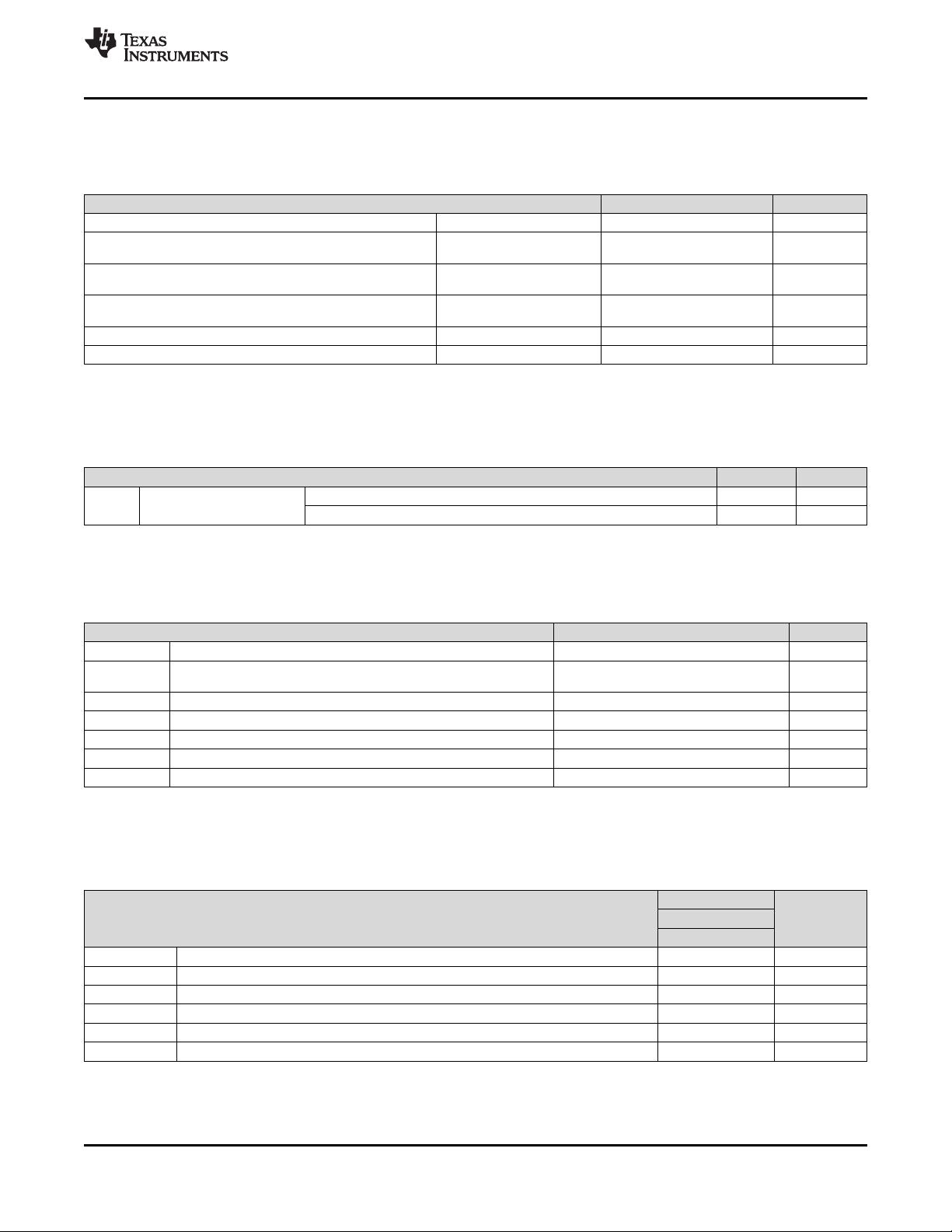
没有合适的资源?快使用搜索试试~ 我知道了~
TI-CDCE6214.pdf
需积分: 10 0 下载量 166 浏览量
2022-11-30
13:01:38
上传
评论 4
收藏 6.04MB PDF 举报
温馨提示
![preview](https://dl-preview.csdnimg.cn/87216420/0001-e5c4aa3b755eec88a18c158fd63b60c9_thumbnail.jpeg)
![preview-icon](https://csdnimg.cn/release/downloadcmsfe/public/img/scale.ab9e0183.png)
试读
55页
TI-CDCE6214.pdf
资源推荐
资源详情
资源评论
![zip](https://img-home.csdnimg.cn/images/20210720083736.png)
![rar](https://img-home.csdnimg.cn/images/20210720083606.png)
![zip](https://img-home.csdnimg.cn/images/20210720083736.png)
![pdf](https://img-home.csdnimg.cn/images/20210720083512.png)
![zip](https://img-home.csdnimg.cn/images/20210720083736.png)
![pdf](https://img-home.csdnimg.cn/images/20210720083512.png)
![](https://csdnimg.cn/release/download_crawler_static/87216420/bg1.jpg)
DAC
FPGA
LVCMOS
Crystal Copy
DAC
Ethernet
Voltage Domain
1.8V / 2.5V / 3.3V
Voltage Domain
1.8V / 2.5V / 3.3V
Voltage Domain
1.8V / 2.5V / 3.3V
Crystal
CDCE6214
PCIe
MCU
Product
Folder
Order
Now
Technical
Documents
Tools &
Software
Support &
Community
An IMPORTANT NOTICE at the end of this data sheet addresses availability, warranty, changes, use in safety-critical applications,
intellectual property matters and other important disclaimers. PRODUCTION DATA.
CDCE6214
SNAS811 –JULY 2020
CDCE6214 Ultra-Low Power Clock Generator With One PLL, Four Differential Outputs,
Two Inputs, and Internal EEPROM
1
1 Features
1
• Configurable high performance, low-power, frac-N
PLL with RMS jitter with spurs (12 kHz – 20 MHz,
F
out
> 100 MHz) as:
– Integer mode:
– Differential output: 350 fs typical, 600 fs
maximum
– LVCMOS output: 1.05 ps typical, 1.5 ps
maximum
– Fractional mode:
– Differential output: 1.7 ps typical, 2.1 ps
maximum
– LVCMOS output: 2.0 ps typical, 4.0 ps
maximum
• Supports PCIe Gen1/2/3/4 with SSC and Gen
1/2/3/4/5 without SSC
• 2.335-GHz to 2.625-GHz internal VCO
• Typical power consumption: 65 mA for 4-output
channel, 23 mA for 1-output channel.
• Universal clock input, two reference inputs for
redundancy
– Differential AC-coupled or LVCMOS: 10 MHz
to 200 MHz
– Crystal: 10 MHz to 50 MHz
• Flexible output clock distribution
– 4 channel dividers: Up to 5 unique output
frequencies from 24 kHz to 328.125 MHz
– Combination of LVDS-like, LP-HCSL or
LVCMOS outputs on OUT0 – OUT4 pins
– Glitchless output divider switching and output
channel synchronization
– Individual output enable through GPIO and
register
• Frequency margining options
– DCO mode: frequency increment/decrement
with 10ppb or less step-size
• Fully-integrated, configurable loop bandwidth: 100
kHz to 1.6 MHz
• Single or mixed supply for level translation: 1.8
V/2.5 V/3.3 V
• Configurable GPIOs and flexible configuration
options
– I
2
C-compatible interface: up to 400 kHz
– Integrated EEPROM with two pages and
external select pin. In-situ programming
allowed.
• Supports 100-Ω systems
• Low electromagnetic emissions
• Small footprint: 24-pin VQFN (4 mm × 4 mm)
2 Applications
• PCIe Gen 1 - Gen 5 clocking
• Data Center & Enterprise Computing, PC &
Notebook
• Enterprise Machine - Multi-Function Printer
• Test & Measurement, Handheld Equipment
3 Description
The CDCE6214 is a four-channel, ultra-low power,
medium grade jitter, clock generator that can
generate five independent clock outputs selectable
between various modes of drivers. The input source
could be a single-ended or differential input clock
source, or a crystal. The CDCE6214 features a frac-N
PLL to synthesize unrelated base frequency from any
input frequency. The CDCE6214 can be configured
through the I
2
C interface. In the absence of the serial
interface, the GPIO pins can be used in Pin Mode to
configure the product into distinctive configurations.
Device Information
(1)
PART NUMBER PACKAGE BODY SIZE (NOM)
CDCE6214 VQFN (24) 4.00 mm × 4.00 mm
(1) For all available packages, see the orderable addendum at
the end of the data sheet.
Application Example CDCE6214
![](https://csdnimg.cn/release/download_crawler_static/87216420/bg2.jpg)
2
CDCE6214
SNAS811 –JULY 2020
www.ti.com
Product Folder Links: CDCE6214
Submit Documentation Feedback Copyright © 2020, Texas Instruments Incorporated
Table of Contents
1 Features.................................................................. 1
2 Applications ........................................................... 1
3 Description ............................................................. 1
4 Revision History..................................................... 2
5 Description (cont.)................................................. 3
6 Pin Configuration and Functions......................... 3
7 Specifications......................................................... 5
7.1 Absolute Maximum Ratings ...................................... 5
7.2 ESD Ratings.............................................................. 5
7.3 Recommended Operating Conditions....................... 5
7.4 Thermal Information.................................................. 5
7.5 EEPROM Characteristics.......................................... 6
7.6 Reference Input, Single-Ended Characteristics........ 6
7.7 Reference Input, Differential Characteristics ............ 6
7.8 Reference Input, Crystal Mode Characteristics ........ 6
7.9 General-Purpose Input Characteristics..................... 6
7.10 Triple Level Input Characteristics............................ 7
7.11 Logic Output Characteristics................................... 7
7.12 Phase Locked Loop Characteristics ....................... 7
7.13 Closed-Loop Output Jitter Characteristics .............. 7
7.14 Input and Output Isolation....................................... 8
7.15 Buffer Mode Characteristics.................................... 8
7.16 PCIe Spread Spectrum Generator.......................... 8
7.17 LVCMOS Output Characteristics ............................ 9
7.18 LP-HCSL Output Characteristics ............................ 9
7.19 LVDS Output Characteristics ................................ 10
7.20 Output Synchronization Characteristics................ 10
7.21 Power-On Reset Characteristics........................... 10
7.22 I
2
C-Compatible Serial Interface Characteristics.... 10
7.23 Timing Requirements, I
2
C-Compatible Serial
Interface ................................................................... 11
7.24 Power Supply Characteristics ............................... 11
7.25 Typical Characteristics.......................................... 12
8 Parameter Measurement Information ................ 14
8.1 Reference Inputs..................................................... 14
8.2 Outputs.................................................................... 14
8.3 Serial Interface........................................................ 15
8.4 PSNR Test .............................................................. 15
8.5 Clock Interfacing and Termination .......................... 16
9 Detailed Description............................................ 18
9.1 Overview ................................................................. 18
9.2 Functional Block Diagram ....................................... 18
9.3 Feature Description................................................. 18
9.4 Device Functional Modes........................................ 30
9.5 Programming........................................................... 30
10 Application and Implementation........................ 38
10.1 Application Information.......................................... 38
10.2 Typical Application ............................................... 39
11 Power Supply Recommendations ..................... 40
11.1 Power-Up Sequence............................................. 40
11.2 Decoupling ............................................................ 40
12 Layout................................................................... 41
12.1 Layout Guidelines ................................................. 41
12.2 Layout Examples................................................... 41
13 Device and Documentation Support ................. 43
13.1 Device Support .................................................... 43
13.2 Receiving Notification of Documentation Updates 43
13.3 Support Resources ............................................... 43
13.4 Trademarks........................................................... 43
13.5 Electrostatic Discharge Caution............................ 43
13.6 Glossary................................................................ 43
14 Mechanical, Packaging, and Orderable
Information ........................................................... 43
4 Revision History
NOTE: Page numbers for previous revisions may differ from page numbers in the current version.
DATE REVISION NOTES
July 2020 * Initial release.
![](https://csdnimg.cn/release/download_crawler_static/87216420/bg3.jpg)
24 VDD_VCO7OUT0
1SECREF_P 18 OUT2_P
23 HW_SW_CTRL8PDN
2SECREF_N 17 OUT2_N
22 OUT1_P9OUT4_N
3VDD_REF 16 VDDO_12
21 OUT1_N10OUT4_P
4REFSEL 15 VDDO_34
20 GPIO111GPIO4
5PRIREF_P 14 OUT3_P
19 SDA/GPIO212SCL/GPIO3
6PRIREF_N 13 OUT3_N
Not to scale
DAP
3
CDCE6214
www.ti.com
SNAS811 –JULY 2020
Product Folder Links: CDCE6214
Submit Documentation FeedbackCopyright © 2020, Texas Instruments Incorporated
(1) G = Ground, P = Power
(2) I = Input, I/O = Input/Output, O = Output
(3) I, R
PUPD
= Input with Resistive Pull-up and Pull-down
(4) I, R
PU
= Input with Resistive Pull=up
(5) I/O, R
PU
= Input/Output with resistive pull-up
5 Description (cont.)
On-chip EEPROM can be used to change the configuration, which is pre-selectable through the pins. The device
provides frequency margining options with glitch-free operation to support system design verification tests (DVT)
and Ethernet Audio-Video Bridging (eAVB). Fine frequency margining is available on any output channel by
steering the fractional feedback divider in DCO mode.
Internal power conditioning provides excellent power supply ripple rejection (PSRR), reducing the cost and
complexity of the power delivery network. The analog and digital core blocks operate from either a 1.8-V, 2.5-V,
or 3.3-V ±5% supply, and output blocks operate from a 1.8-V, 2.5-V, or 3.3-V ±5% supply.
The CDCE6214 enables high-performance clock trees from a single reference at ultra-low power with a small
footprint. The factory- and user-programmable EEPROM features make the CDCE6214 an easy-to-use, instant-
on clocking device with a low power consumption.
6 Pin Configuration and Functions
CDCE6214 RGE Package
24-Pin VQFN
Top View
Pin Functions
(1) (2) (3) (4) (5)
PIN
I/O DESCRIPTION
NAME NO.
POWER
DAP — G
Die Attach Pad. The DAP is an electrical connection and provides a thermal dissipation path.
For proper electrical and thermal performance of the device, the DAP must be connected to
PCB ground plane.
VDD_REF 3 P 1.8 V/2.5 V/3.3 V Power Supply for Reference Input and Digital.
VDD_VCO 24 P 1.8 V/2.5 V/3.3 V Power Supply for PLL/VCO.
![](https://csdnimg.cn/release/download_crawler_static/87216420/bg4.jpg)
4
CDCE6214
SNAS811 –JULY 2020
www.ti.com
Product Folder Links: CDCE6214
Submit Documentation Feedback Copyright © 2020, Texas Instruments Incorporated
Pin Functions
(1) (2) (3) (4) (5)
(continued)
PIN
I/O DESCRIPTION
NAME NO.
VDDO_12 16 P 1.8 V/2.5 V/3.3 V Power Supply for OUT1 and OUT2 channels
VDDO_34 15 P 1.8 V/2.5 V/3.3 V Power Supply for OUT0, OUT3, and OUT4 channels
INPUT BLOCK
HW_SW_CT
RL
23 I, R
PUPD
Manual selection pin for EEPROM pages (3-state). Weak Pullup/Pulldown. R
PU
= 50 kΩ. R
PD
= 50 kΩ.
PRIREF_P 5 I Primary reference clock. Accepts a differential or single-ended input. Input pins need AC-
coupling capacitors and internally biased in differential mode. For LVCMOS, input should be
provided on PRIREF_P and the non-driven input pin should be pulled down to ground.
Internal biasing for differential mode is disabled in single-ended mode.
PRIREF_N 6 I
REFSEL 4 I, R
PUPD
Manual selection pin of reference input (3-state). Weak Pullup/Pulldown. R
PU
= 50 kΩ. R
PD
=
50 kΩ.
SECREF_P 1 I Secondary reference clock. Accepts a differential or single-ended input or XTAL. Input pins
need AC-coupling capacitors and internally biased in differential mode. For XTAL input,
connect crystal between SECREF_P and SECREF_N pin. SECREF_P is XOUT, SECREF_N
is XIN. This device do not need any power limiting resistor on XOUT. For LVCMOS input,
input should be provided on SECREF_P, and the non-driven input pin should be pulled down
to ground. Internal biasing for differential mode is disabled in single-ended and XTAL mode.
SECREF_N 2 I
OUTPUT BLOCK
OUT0
7 O
LVCMOS Output 0. Reference Input can be bypassed into this output. Output slew-rate
configurable on all LVCMOS outputs.
OUT1_P 22 O
LVDS-like/LP-HCSL/LVCMOS Output Pair 1. Programmable driver with LVDS-like/LP-HCSL
or 2x LVCMOS outputs.
OUT1_N 21 O
OUT2_P 18 O
LVDS-like/LP-HCSL Output Pair 2. Programmable driver with LVDS-like/LP-HCSL outputs.
OUT2_N 17 O
OUT3_P 14 O
LVDS-like/LP-HCSL Output Pair 3. Programmable driver with LVDS-like/LP-HCSL outputs.
OUT3_N 13 O
OUT4_P 10 O
LVDS-like/LP-HCSL/LVCMOS Output Pair 4. Programmable driver with LVDS-like/LP-HCSL
or 2x LVCMOS outputs.
OUT4_N 9 O
DIGITAL CONTROL / INTERFACES
GPIO1 20 I/O, R
PU
STATUS output or GPIO1 input. Weak pullup resistor when configured as Input. R
PU
= 50
kΩ. Pullup resistor disabled in output mode.
GPIO4 11 I/O, R
PU
STATUS output or GPIO4 input. Weak pullup resistor when configured as Input. R
PU
= 50
kΩ. Pullup resistor disabled in output mode.
PDN 8 I, R
PU
Device Power-down/RESET (active low) or SYNCN. Weak pullup resistor. R
PU
= 50 kΩ.
Pullup resistor disabled in output mode.
SDA/GPIO2 19 I/O
I
2
C Serial Data (bidirectional, open-drain) or GPIO2 input. Requires an external pullup
resistor to VDD_REF in I
2
C mode. I
2
C slave address is initialized from on-chip EEPROM.
Fail-safe Input.
SCL/GPIO3 12 I
I
2
C Serial Clock or GPIO3 input. Requires an external pullup resistor to VDD_REF in I
2
C
mode. Fail-safe Input.
![](https://csdnimg.cn/release/download_crawler_static/87216420/bg5.jpg)
5
CDCE6214
www.ti.com
SNAS811 –JULY 2020
Product Folder Links: CDCE6214
Submit Documentation FeedbackCopyright © 2020, Texas Instruments Incorporated
(1) Stresses beyond those listed under Absolute Maximum Ratings may cause permanent damage to the device. These are stress ratings
only, which do not imply functional operation of the device at these or any other conditions beyond those indicated under Recommended
Operating Conditions. Exposure to absolute-maximum-rated conditions for extended periods may affect device reliability.
(2) VDDO_X refers to the output supply for a specific output channel, where X denotes the channel index.
7 Specifications
7.1 Absolute Maximum Ratings
over operating free-air temperature range (unless otherwise noted)
(1)
MIN MAX UNIT
VDD_REF, VDD_VCO, VDDO_12, VDDO_34 Supply Voltage -0.3 3.63 V
PRIREF_P, PRIREF_N, SECREF_P, SECREF_N Input Voltage -0.3
VDD_REF +
0.3
V
GPIO1, SDA/GPIO2, SCL/GPIO3, GPIO4, REFSEL, HW_SW_CTRL,
PDN
Input Voltage -0.3
VDD_REF +
0.3
V
OUT0, OUT1_P, OUT1_N, OUT2_P, OUT2_N, OUT3_P, OUT3_N,
OUT4_P, OUT4_N
(2)
Output Voltage -0.3
VDDO_X
(2)
+
0.3
V
T
J
Junction Temperature 125 ºC
T
stg
Storage temperature -65 150 ºC
(1) JEDEC document JEP155 states that 500-V HBM allows safe manufacturing with a standard ESD control process.
(2) JEDEC document JEP157 states that 250-V CDM allows safe manufacturing with a standard ESD control process.
7.2 ESD Ratings
VALUE UNIT
V
(ESD)
Electrostatic discharge
Human-body model (HBM), per ANSI/ESDA/JEDEC JS-001
(1)
2000 V
Charged-device model (CDM), per JEDEC specification JESD22-C101
(2)
750 V
(1) VDD pin should monotonically reach 95% of its final value within supply ramp time. All VDD pins were tied together for this evaluation.
For non-monotonic or slower power supply ramp, it is recommended to pull-down PDN pin until VDD pins have reached 95% of its final
value. PDN pin has a 50 kΩ pullup resistor. When PDN pin cannot be actively controlled, TI recommends to add a capacitor to GND on
PDN pin to delay the release of reset.
7.3 Recommended Operating Conditions
over operating free-air temperature range (unless otherwise noted)
MIN NOM MAX UNIT
VDD_VCO Core supply voltage 1.71 1.8, 2.5, 3.3 3.465 V
VDDO_12,
VDDO_34
Output supply voltage 1.71 1.8, 2.5, 3.3 3.465 V
VDD_REF Reference supply voltage 1.71 1.8, 2.5, 3.3 3.465 V
T
A
Ambient temperature -40 105 ºC
T
J
Junction temperature -40 125 ºC
T
LOCK
Continuous lock over temperature (without VCO calibration) 145 ºC
t
RAMP
Maximum supply voltage ramp time
(1)
0.1 30 ms
(1) For more information about traditional and new thermal metrics, see the Semiconductor and IC Package Thermal Metrics application
report, SPRA953.
7.4 Thermal Information
THERMAL METRIC
(1)
CDCE6214-Q1
UNITRGE (VQFN)
24 PINS
R
θJA
Junction-to-ambient thermal resistance 32.5 °C/W
R
θJC(top)
Junction-to-case (top) thermal resistance 32.5 °C/W
R
θJB
Junction-to-board thermal resistance 12.2 °C/W
R
θJC(bot)
Junction-to-case (bottom) thermal resistance 2.0 °C/W
ψ
JT
Junction-to-top characterization parameter 0.4 °C/W
ψ
JB
Junction-to-board characterization parameter 12.2 °C/W
剩余54页未读,继续阅读
资源评论
![avatar-default](https://csdnimg.cn/release/downloadcmsfe/public/img/lazyLogo2.1882d7f4.png)
![avatar](https://profile-avatar.csdnimg.cn/107303f5121d47e49d12d0a9ae68af10_weixin_54787054.jpg!1)
不觉明了
- 粉丝: 3242
- 资源: 5614
上传资源 快速赚钱
我的内容管理 展开
我的资源 快来上传第一个资源
我的收益
登录查看自己的收益我的积分 登录查看自己的积分
我的C币 登录后查看C币余额
我的收藏
我的下载
下载帮助
![voice](https://csdnimg.cn/release/downloadcmsfe/public/img/voice.245cc511.png)
![center-task](https://csdnimg.cn/release/downloadcmsfe/public/img/center-task.c2eda91a.png)
最新资源
- 华为HCIA-WLAN 3.0 课程视频(45 STA无法上线故障排查.mp4)
- 华为HCIA-WLAN 3.0 课程视频(44 AP无法上线故障排查(下).mp4)
- 华为HCIA-WLAN 3.0 课程视频(43 AP无法上线故障排查(上).mp4)
- python实现基于U-net和MRI图像的膀胱壁边缘以及膀胱肿瘤检测(高准确率)+源码+开发文档+模型训练(毕业设计&课程设计
- 华为HCIA-WLAN 3.0 课程视频(42 WLAN系统维护的方法及故障处理命令.mp4)
- 华为HCIA-WLAN 3.0 课程视频(41 WLAN故障处理一般流程(下).mp4)
- C++基于OpenCV+Qt的人脸识别考勤系统-毕业设计+源代码+文档说明.zip
- python爬虫资源下载
- 华为HCIA-WLAN 3.0 课程视频(40 WLAN故障处理一般流程(上).mp4)
- PHP教材管理系统设计(源码+数据库)
资源上传下载、课程学习等过程中有任何疑问或建议,欢迎提出宝贵意见哦~我们会及时处理!
点击此处反馈
![feedback](https://img-home.csdnimg.cn/images/20220527035711.png)
![feedback-tip](https://img-home.csdnimg.cn/images/20220527035111.png)
安全验证
文档复制为VIP权益,开通VIP直接复制
![dialog-icon](https://csdnimg.cn/release/downloadcmsfe/public/img/green-success.6a4acb44.png)