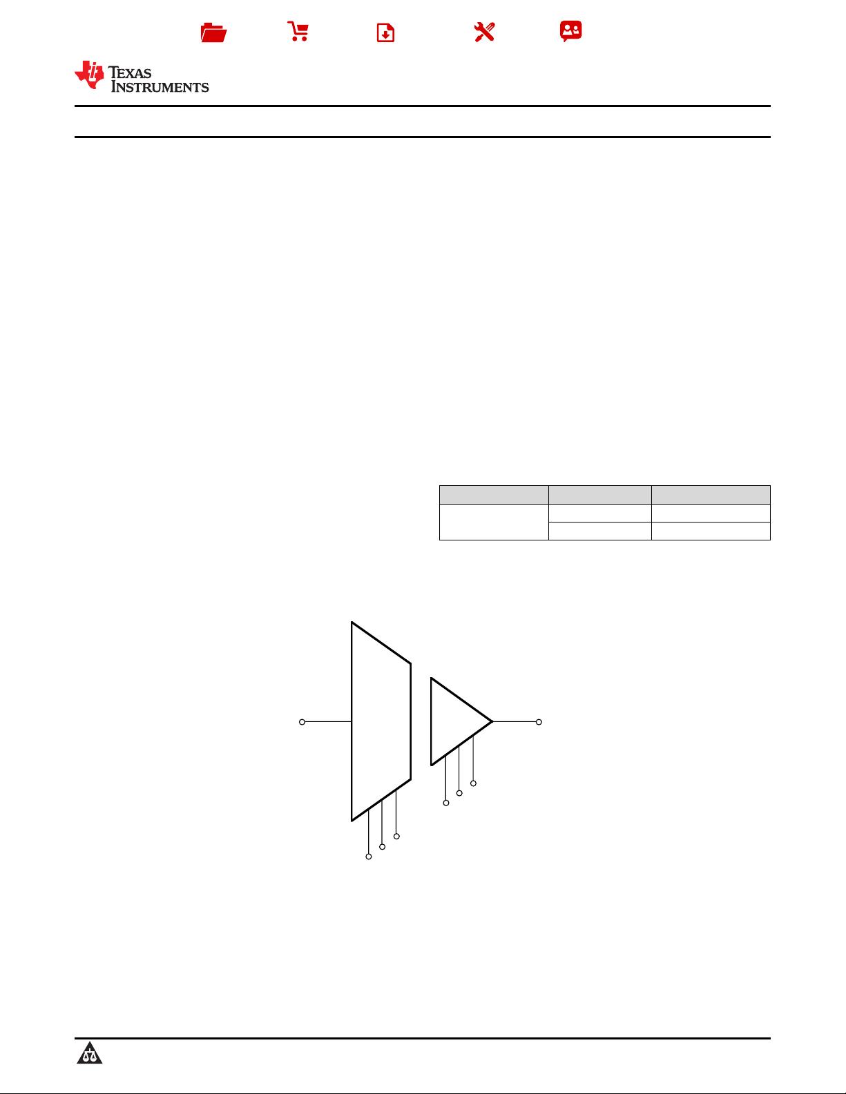
没有合适的资源?快使用搜索试试~ 我知道了~
TI-ISO122.pdf
需积分: 9 0 下载量 32 浏览量
2022-11-29
23:28:46
上传
评论 4
收藏 1.09MB PDF 举报
温馨提示
![preview](https://dl-preview.csdnimg.cn/87213111/0001-e35008361cacd805048550dfc186c19b_thumbnail.jpeg)
![preview-icon](https://csdnimg.cn/release/downloadcmsfe/public/img/scale.ab9e0183.png)
试读
26页
TI-ISO122.pdf
资源推荐
资源详情
资源评论
![](https://csdnimg.cn/release/download_crawler_static/87213111/bg1.jpg)
V
OUT
V
IN
+V
S1
–V
S1
Gnd
+V
S2
–V
S2
Gnd
Product
Folder
Sample &
Buy
Technical
Documents
Tools &
Software
Support &
Community
ISO122
SBOS160A –NOVEMBER 1993–REVISED JANUARY 2015
ISO122 Precision Lowest-Cost Isolation Amplifier
1 Features 3 Description
The ISO122 is a precision isolation amplifier
1
• 100% Tested for High-Voltage Breakdown
incorporating a novel duty cycle modulation-
• Rated 1500 Vrms
demodulation technique. The signal is transmitted
• High IMR: 140 dB at 60 Hz
digitally across a 2-pF differential capacitive barrier.
With digital modulation the barrier characteristics do
• Bipolar Operation: V
O
= ±10 V
not affect signal integrity, thus resulting in excellent
• 16-Pin Plastic DIP and 28-Lead SOIC
reliability and good high-frequency transient immunity
• Ease of Use: Fixed Unity Gain Configuration
across the barrier. Both barrier capacitors are
imbedded in the plastic body of the package.
• 0.020% Maximum Nonlinearity
• ±4.5-V to ±18-V Supply Range
The ISO122 is easy to use. No external components
are required for operation. The key specifications are
2 Applications
0.020% maximum nonlinearity, 50-kHz signal
bandwidth, and 200-V/°C V
OS
drift. A power supply
• Industrial Process Control:
range of 4.5 V to 18 V and quiescent currents of 5
– Transducer Isolator, Isolator for
mA on V
S1
and ±5.5 mA on V
S2
make the ISO122
Thermocouples, RTDs, Pressure Bridges, and
ideal for a wide range of applications.
Flow Meters, 4-mA to 20-mA Loop Isolation
The ISO122 is available in 16-pin plastic DIP and
• Ground Loop Elimination
28-lead plastic surface-mount packages.
• Motor and SCR Control
Device Information
(1)
• Power Monitoring
PART NUMBER PACKAGE BODY SIZE (NOM)
• PC-Based Data Acquisition
PDIP (16) 17.90 mm × 7.50 mm
• Test Equipment
ISO122
SOIC (28) 20.01 mm × 6.61 mm
(1) For all available packages, see the orderable addendum at
the end of the data sheet.
4 Simplified Schematic
1
An IMPORTANT NOTICE at the end of this data sheet addresses availability, warranty, changes, use in safety-critical applications,
intellectual property matters and other important disclaimers. PRODUCTION DATA.
![](https://csdnimg.cn/release/download_crawler_static/87213111/bg2.jpg)
ISO122
SBOS160A –NOVEMBER 1993–REVISED JANUARY 2015
www.ti.com
Table of Contents
8.3 Feature Description................................................... 8
1 Features.................................................................. 1
8.4 Device Functional Modes.......................................... 9
2 Applications ........................................................... 1
9 Application and Implementation .......................... 9
3 Description ............................................................. 1
9.1 Application Information.............................................. 9
4 Simplified Schematic............................................. 1
9.2 Typical Application ................................................. 10
5 Revision History..................................................... 2
10 Power Supply Recommendations ..................... 17
6 Pin Configuration and Functions......................... 3
10.1 Signal and Supply Connections............................ 17
7 Specifications......................................................... 4
11 Layout................................................................... 18
7.1 Absolute Maximum Ratings ...................................... 4
11.1 Layout Guidelines ................................................. 18
7.2 ESD Ratings.............................................................. 4
11.2 Layout Example .................................................... 18
7.3 Recommended Operating Conditions....................... 4
12 Device and Documentation Support ................. 19
7.4 Thermal Information.................................................. 4
12.1 Trademarks........................................................... 19
7.5 Electrical Characteristics........................................... 5
12.2 Electrostatic Discharge Caution............................ 19
7.6 Typical Characteristics.............................................. 6
12.3 Glossary................................................................ 19
8 Detailed Description .............................................. 8
13 Mechanical, Packaging, and Orderable
8.1 Overview ................................................................... 8
Information ........................................................... 19
8.2 Functional Block Diagram ......................................... 8
5 Revision History
Changes from Original (November1993) to Revision A Page
• Added Pin Configuration and Functions section, ESD Ratings table, Feature Description section, Device Functional
Modes, Application and Implementation section, Power Supply Recommendations section, Layout section, Device
and Documentation Support section, and Mechanical, Packaging, and Orderable Information section ............................... 1
2 Submit Documentation Feedback Copyright © 1993–2015, Texas Instruments Incorporated
Product Folder Links: ISO122
![](https://csdnimg.cn/release/download_crawler_static/87213111/bg3.jpg)
1
2
16
15
10
9
7
8
+V
S1
–V
S1
V
OUT
Gnd 2
Gnd 1
V
IN
–V
S2
+V
S2
1
2
28
27
16
15
13
14
+V
S1
–V
S1
V
OUT
Gnd 2
Gnd 1
V
IN
–V
S2
+V
S2
ISO122
www.ti.com
SBOS160A –NOVEMBER 1993–REVISED JANUARY 2015
6 Pin Configuration and Functions
16 Pins PDIP 28 Pins SOIC
NVF Package DVA Package
Top View Top View
Pin Functions
PIN
I/O DESCRIPTION
NAME PDIP SOIC
GND 8 14 - Low-side ground reference
GND 16 28 - High-side ground reference
V
IN
15 27 I High-side analog input
V
OUT
7 13 O Low-side analog output
+V
S1
1 1 - High-side positive analog supply
-V
S1
2 2 - High-side negative analog supply
+V
S2
9 15 - Low-side positive analog supply
-V
S2
10 16 - Low-side negative analog supply
Copyright © 1993–2015, Texas Instruments Incorporated Submit Documentation Feedback 3
Product Folder Links: ISO122
![](https://csdnimg.cn/release/download_crawler_static/87213111/bg4.jpg)
ISO122
SBOS160A –NOVEMBER 1993 –REVISED JANUARY 2015
www.ti.com
7 Specifications
7.1 Absolute Maximum Ratings
over operating free-air temperature range (unless otherwise noted)
(1)
MIN MAX UNIT
Supply voltage ±18 V
V
IN
100 V
Continuous isolation voltage 1500 Vrms
Junction temperature 150 °C
Output short to common Continuous
Storage temperature, T
stg
–40 125 °C
(1) Stresses beyond those listed under Absolute Maximum Ratings may cause permanent damage to the device. These are stress ratings
only, which do not imply functional operation of the device at these or any other conditions beyond those indicated under Recommended
Operating Conditions. Exposure to absolute-maximum-rated conditions for extended periods may affect device reliability.
7.2 ESD Ratings
VALUE UNIT
Human body model (HBM), per ANSI/ESDA/JEDEC JS-001
(1)
±1000
V
(ESD)
Electrostatic discharge V
Charged-device model (CDM), per JEDEC specification JESD22- ±500
C101
(2)
(1) JEDEC document JEP155 states that 500-V HBM allows safe manufacturing with a standard ESD control process.
(2) JEDEC document JEP157 states that 250-V CDM allows safe manufacturing with a standard ESD control process.
7.3 Recommended Operating Conditions
over operating free-air temperature range (unless otherwise noted)
MIN NOM MAX UNIT
TA –25 85 °C
+VS1 15
-VS1 –15
+VS2 15
-VS2 –15
VIN ±10
7.4 Thermal Information
ISO122
THERMAL METRIC
(1)
NVF (PDIP) DVA (SOIC) UNIT
16 PINS 28 PINS
R
θJA
Junction-to-ambient thermal resistance 51.0 79.8
R
θJC(top)
Junction-to-case (top) thermal resistance 32.4 32.9
R
θJB
Junction-to-board thermal resistance 29.5 42.2 °C/W
ψ
JT
Junction-to-top characterization parameter 10.4 6.6
ψ
JB
Junction-to-board characterization parameter 29.0 40.9
(1) For more information about traditional and new thermal metrics, see the IC Package Thermal Metrics application report, SPRA953.
4 Submit Documentation Feedback Copyright © 1993–2015, Texas Instruments Incorporated
Product Folder Links: ISO122
![](https://csdnimg.cn/release/download_crawler_static/87213111/bg5.jpg)
ISO122
www.ti.com
SBOS160A –NOVEMBER 1993–REVISED JANUARY 2015
7.5 Electrical Characteristics
At T
A
= +25°C , V
S1
= V
S2
= ±15 V, and R
L
= 2 kΩ, unless otherwise noted.
ISO122P/U ISO122JP/JU
TEST
PARAMETER UNIT
CONDITIONS
MIN TYP MAX MIN TYP MAX
ISOLATION
Voltage rated continuous ac 60Hz 1500 1500 Vac
100% Test
(1)
1s, 5pc PD 2400 2400 Vac
Isolation Mode Rejection 60Hz 140 140 dB
Barrier Impedance 10
14
|| 2 10
14
|| 2 Ω || pF
Leakage Current at 60Hz V
ISO
= 240Vrms 0.18 0.5 0.18 0.5 µArms
GAIN
Nominal Gain 1 1 V/V
V
O
= ±10V
Gain Error ±0.05 ±0.50 ±0.05 ±0.50 %FSR
Gain vs Temperature ±10 ±10 ppm/°C
Nonlinearity
(2)
±0.016 ±0.020 ±0.025 ±0.050 %FSR
INPUT OFFSET VOLTAGE
Initial Offset ±20 ±50 ±20 ±50 mV
vs Temperature ±200 ±200 µV/°C
vs Supply ±2 ±2 mV/V
Noise 4 µV/√Hz
INPUT
Voltage Range ±10 ±12.5 ±10 ±12.5 V
Resistance 200 200 kΩ
OUTPUT
Voltage Range ±10 ±12.5 ±10 ±12.5 V
Current Drive ±5 ±15 ±5 ±15 mA
Capacitive Load Drive 0.1 0.1 µF
Ripple Voltage
(3)
20 20 mVp-p
FREQUENCY RESPONSE
Small-Signal Bandwidth 50 50 kHz
Slew Rate 2 2 V/µs
Settling Time 0.10% 50 50 µs
V
O
= ±10V
Settling Time 0.01% 350 350 µs
Overload Recovery Time 150 150 µs
POWER SUPPLIES
Rated Voltage ±15 ±15 V
Voltage Range ±4.5 ±18 ±4.5 ±18 V
V
S1
±5 ±7 ±5 ±7
Quiescent Current mA
V
S2
±5.5 ±7 ±5.5 ±7
TEMPERATURE RANGE
Specification –25 85 –25 85 °C
Operating –25 85 –25 85 °C
Storage –40 125 –40 125 °C
θ
JA
100 100 °C/W
Thermal Resistance
θ
JC
65 65 °C/W
(1) Tested at 1.6 X rated, fail on 5pC partial discharge.
(2) Nonlinearity is the peak deviation of the output voltage from the best-fit straight line. It is expressed as the ratio of deviation to FSR.
(3) Ripple frequency is at carrier frequency (500kHz).
Copyright © 1993–2015, Texas Instruments Incorporated Submit Documentation Feedback 5
Product Folder Links: ISO122
剩余25页未读,继续阅读
资源评论
![avatar-default](https://csdnimg.cn/release/downloadcmsfe/public/img/lazyLogo2.1882d7f4.png)
![avatar](https://profile-avatar.csdnimg.cn/107303f5121d47e49d12d0a9ae68af10_weixin_54787054.jpg!1)
不觉明了
- 粉丝: 3278
- 资源: 5614
上传资源 快速赚钱
我的内容管理 展开
我的资源 快来上传第一个资源
我的收益
登录查看自己的收益我的积分 登录查看自己的积分
我的C币 登录后查看C币余额
我的收藏
我的下载
下载帮助
![voice](https://csdnimg.cn/release/downloadcmsfe/public/img/voice.245cc511.png)
![center-task](https://csdnimg.cn/release/downloadcmsfe/public/img/center-task.c2eda91a.png)
安全验证
文档复制为VIP权益,开通VIP直接复制
![dialog-icon](https://csdnimg.cn/release/downloadcmsfe/public/img/green-success.6a4acb44.png)