TI-BQ24105-Q1.pdf
需积分: 8 3 浏览量
2022-10-29
19:59:30
上传
评论 5
收藏 1.44MB PDF 举报

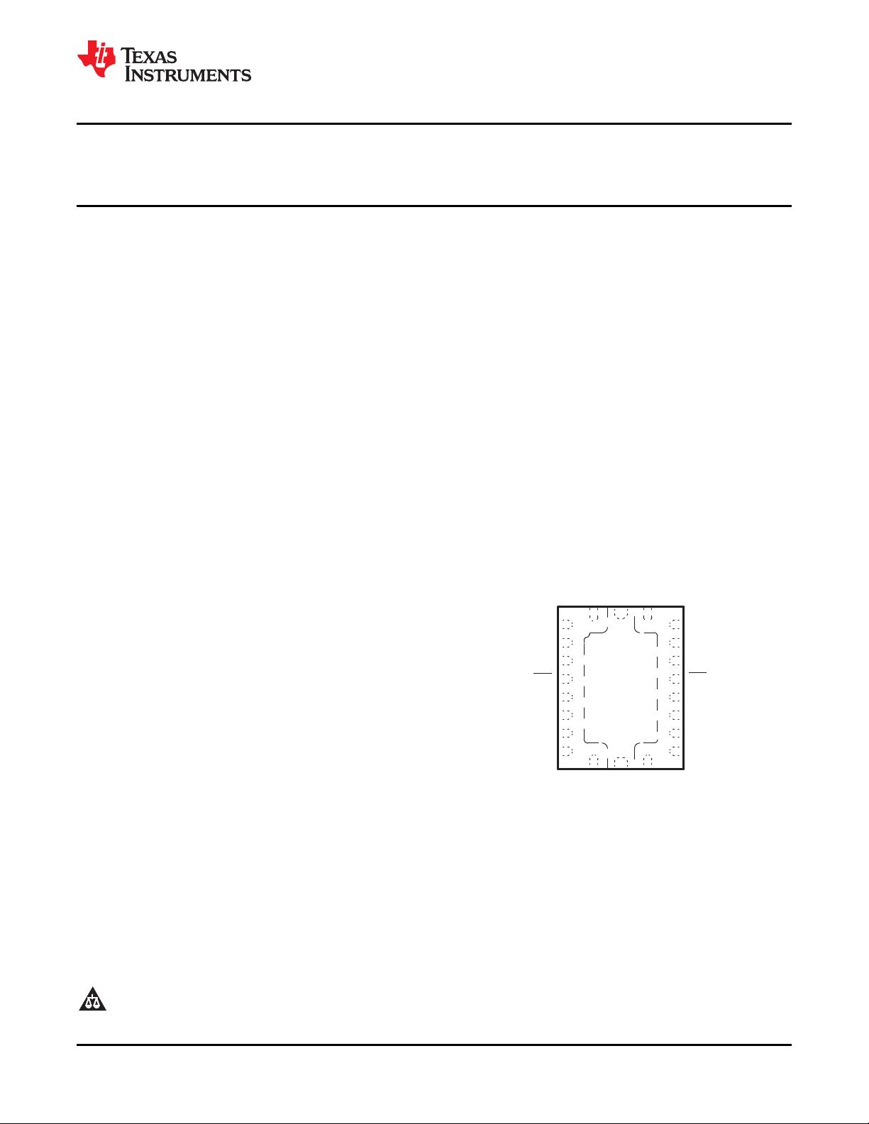
STAT1
IN
IN
PG
VCC
TTC
ISET1
ISET2
STAT2
PGND
PGND
CE
SNS
BAT
FB
TS
OUT
OUT
VTSB
VSS
20
1
11
10
2
3
4
5
6
7
8
9
19
18
17
16
15
14
13
12
bq24105-Q1
www.ti.com
SLUS953A –AUGUST 2009–REVISED APRIL 2012
SYNCHRONOUS SWITCHMODE, LI-ION AND LI-POLYMER CHARGE-MANAGEMENT
IC WITH INTEGRATED POWER FETs ( bqSWITCHER™)
Check for Samples: bq24105-Q1
1
FEATURES
DESCRIPTION
The bqSWITCHER™ series are highly integrated Li-
23
• Qualified for Automotive Applications
ion and Li-polymer switch-mode charge management
• Ideal For Highly Efficient Charger Designs For
devices targeted at a wide range of portable
Single-, Two-, or Three-Cell Li-Ion and Li-
applications. The bqSWITCHER™ series offers
Polymer Battery Packs
integrated synchronous PWM controller and power
FETs, high-accuracy current and voltage regulation,
• Also for LiFePO
4
Battery (see Using bq24105
charge preconditioning, charge status, and charge
to Charge LiFePO4 Battery)
termination, in a small, thermally enhanced QFN
• Integrated Synchronous Fixed-Frequency
package.
PWM Controller Operating at 1.1 MHz
The bqSWITCHER charges the battery in three
With 0% to 100% Duty Cycle
phases: conditioning, constant current, and constant
• Integrated Power FETs For Up To 2-A Charge
voltage. Charge is terminated based on user-
Rate
selectable minimum current level. A programmable
• High-Accuracy Voltage and Current Regulation
charge timer provides a safety backup for charge
termination. The bqSWITCHER automatically restarts
• Stand-Alone (Built-In Charge Management and
the charge cycle if the battery voltage falls below an
Control) Version
internal threshold. The bqSWITCHER automatically
• Status Outputs For LED or Host Processor
enters sleep mode when V
CC
supply is removed.
Interface Indicates Charge-In-Progress, Charge
Completion, Fault, and AC-Adapter Present
RHL PACKAGE
Conditions
(TOP VIEW)
• 20-V Maximum Voltage Rating on IN and OUT
Pins
• High-Side Battery Current Sensing
• Battery Temperature Monitoring
• Automatic Sleep Mode for Low Power
Consumption
• Reverse Leakage Protection Prevents Battery
Drainage
• Thermal Shutdown and Protection
• Built-In Battery Detection
• Available in 20-Pin, 3.5 mm × 4.5 mm, QFN
Package
1
Please be aware that an important notice concerning availability, standard warranty, and use in critical applications of
Texas Instruments semiconductor products and disclaimers thereto appears at the end of this data sheet.
2bqSWITCHER, PowerPAD are trademarks of Texas Instruments.
3All other trademarks are the property of their respective owners.
PRODUCTION DATA information is current as of publication date.
Copyright © 2009–2012, Texas Instruments Incorporated
Products conform to specifications per the terms of the Texas
Instruments standard warranty. Production processing does not
necessarily include testing of all parameters.


剩余37页未读,继续阅读


评论0