没有合适的资源?快使用搜索试试~ 我知道了~
TI-UC2577-ADJ.pdf
需积分: 8 0 下载量 68 浏览量
2022-10-24
22:57:56
上传
评论 5
收藏 366KB PDF 举报
温馨提示
试读
14页
TI-UC2577-ADJ.pdf
资源推荐
资源详情
资源评论
Simple Step-Up Voltage Regulator
•
Requires Few External Components
•
NPN Output Switches 3.0A, 65V(max)
•
Extended Input Voltage Range: 3.0V to 40V
•
Current Mode Operation for Improved
Transient Response, Line Regulation, and
Current Limiting
•
Soft Start Function Provides Controlled
Startup
•
52kHz Internal Oscillator
•
Output Switch Protected by Current Limit,
Undervoltage Lockout and Thermal
Shutdown
•
Improved Replacement for LM2577-ADJ
Series
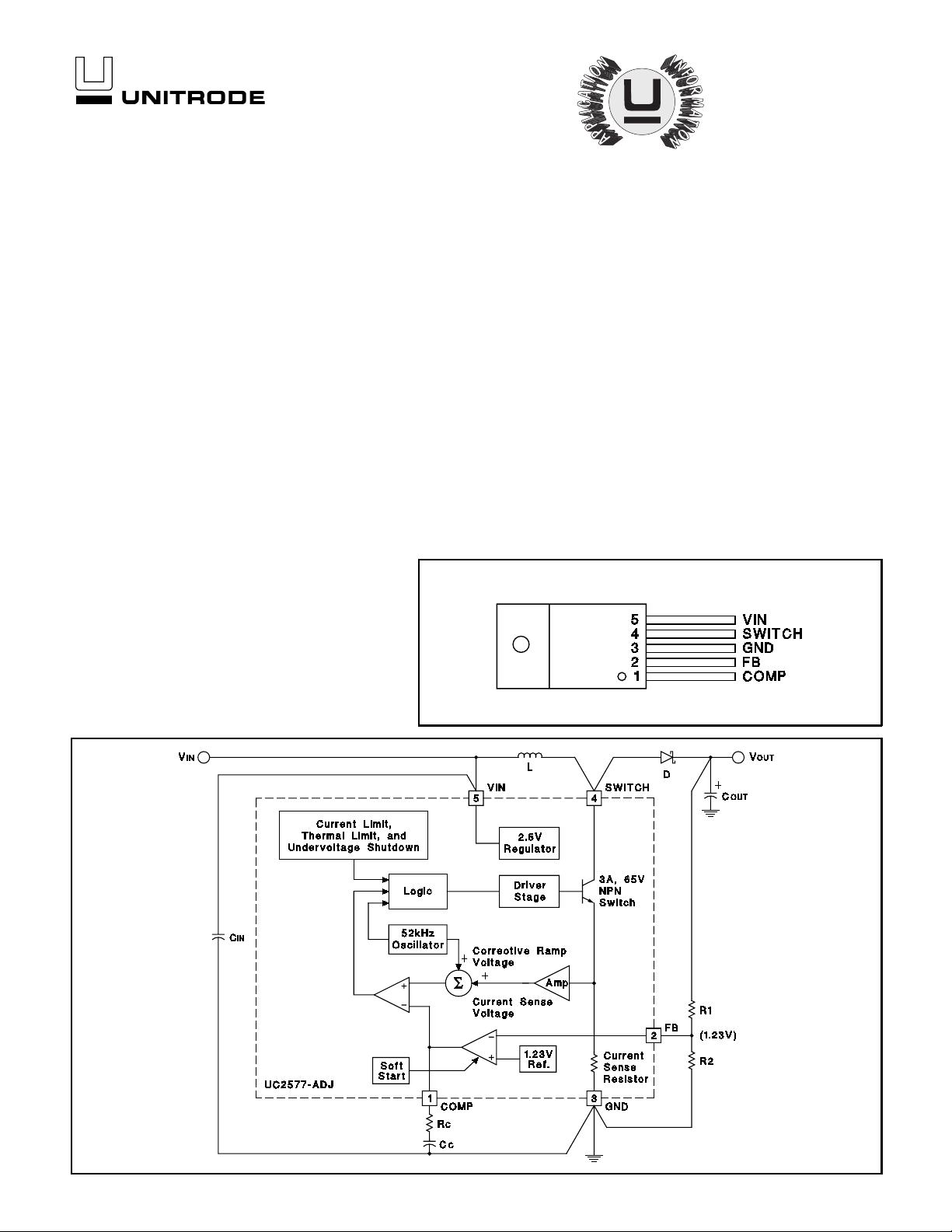
The UC2577-ADJ device provides all the active functions neces-
sary to implement step-up (boost), flyback, and forward converter
switching regulators. Requiring only a few components, these sim-
ple regulators efficiently provide up to 60V as a step-up regulator,
and even higher voltages as a flyback or forward converter regula-
tor.
The UC2577-ADJ features a wide input voltage range of 3.0V to
40V and an adjustable output voltage. An on-chip 3.0A NPN switch
is included with undervoltage lockout, thermal protection circuitry,
and current limiting, as well as soft start mode operation to reduce
current during startup. Other features include a 52kHz fixed fre-
quency on-chip oscillator with no external components and current
mode control for better line and load regulation.
A standard series of inductors and capacitors are available from
several manufacturers optimized for use with these regulators and
are listed in this data sheet.
UC2577-ADJ
3/97
FEATURES DESCRIPTION
CONNECTION DIAGRAM
BLOCK DIAGRAM
UDG-94034
•
Simple Boost and Flyback Converters
•
SEPIC Topology Permits Input Voltage to
be Higher or Lower than Output Voltage
•
Transformer Coupled Forward Regulators
•
Multiple Output Designs
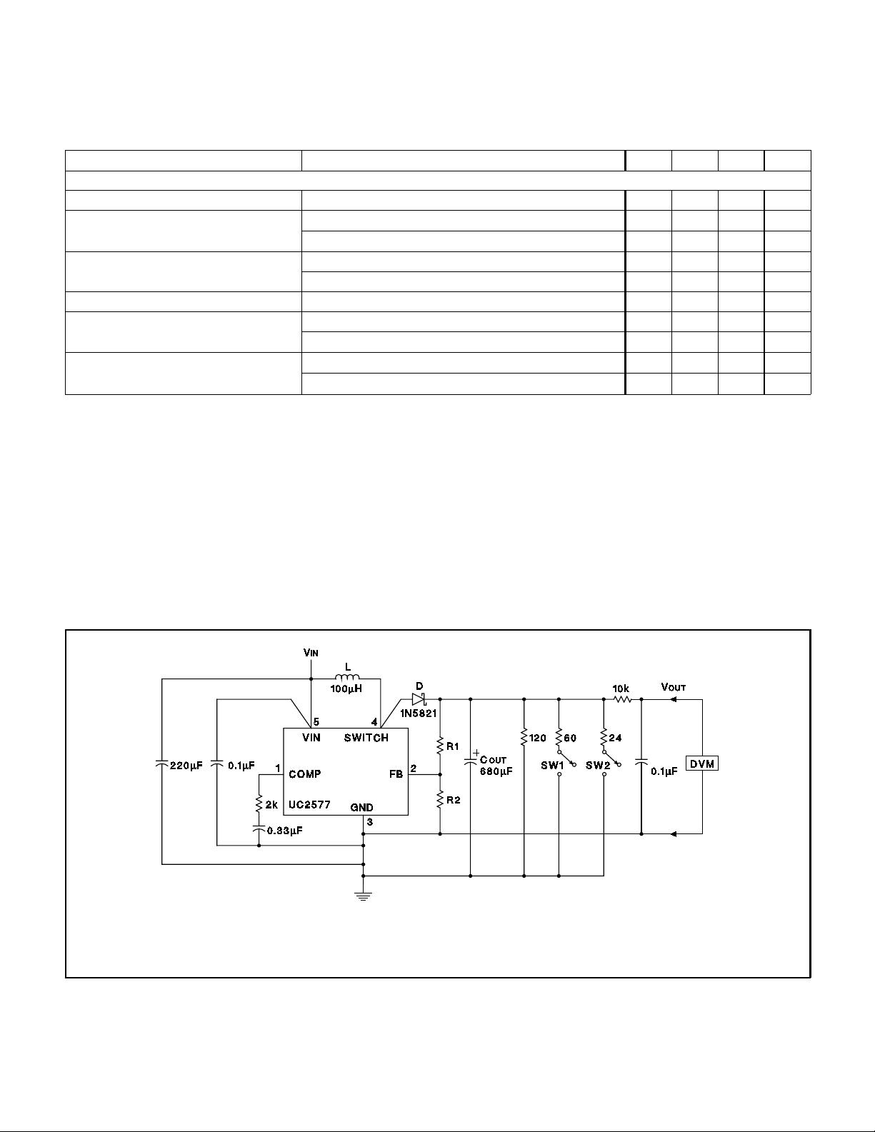
TYPICAL APPLICATIONS
5-Pin TO-220 (Top View)
Also available in TO-263 Package.
PARAMETER TEST CONDITIONS MIN TYP MAX UNITS
System Parameters
Circuit Figure 1
(Note 3)
Output Voltage VIN = 5V to 10V, I
LOAD
= 100mA to 800mA 11.40 12.0 12.60 V
T
J
= 25°C 11.60 12.40 V
Line Regulation VIN = 3.0V to 10V, I
LOAD
= 300mA 20 100 mV
T
J
= 25°C50mV
Load Regulation VIN = 5V, I
LOAD
= 100mA to 800mA 20 100 mV
T
J
= 25°C50mV
Efficiency VIN = 5V, I
LOAD
= 800mA 80 %
Device Parameters
Input Supply Current V
FB
= 1.5V (Switch Off) 7.5 14 mA
T
J
= 25°C10mA
I
SWITCH
= 2.0A, V
COMP
= 2.0V (Max Duty Cycle) 45 85 mA
T
J
= 25°C70mA
Input Supply UVLO I
SWITCH
= 100mA 2.70 2.95 V
T
J
= 25
°
C2.85V
Oscillator Frequency Measured at SWITCH Pin, I
SWITCH
= 100mA 42 52 62 kHz
T
J
= 25°C4856kHz
Reference Voltage Measured at FB Pin, VIN = 3.0V to 40V, V
COMP
= 1.0V 1.206 1.230 1.254 V
T
J
= 25°C 1.214 1.246 V
Reference Voltage Line Regulation VIN = 3.0V to 40V 0.5 mV
Error Amp Input Bias Current V
COMP
= 1.0V 100 800 nA
T
J
= 25
°
C 300 nA
Error Amp Transconductance
I
COMP
= −30µA to +30µA, V
COMP
= 1.0V 1600 3700 5800
µ
mho
T
J
= 25
°
C 2400 4800
µmho
Error Amp Voltage Gain V
COMP
= 0.8V to 1.6V, R
COMP
= 1.0MW (Note 4) 250 800 V/V
T
J
= 25°C 500 V/V
Error Amplifier Output Swing Upper Limit V
FB
= 1.0V 2.0 2.4 V
T
J
= 25
°
C2.2V
Lower Limit V
FB
= 1.5V 0.3 0.55 V
T
J
= 25
°
C0.40V
Error Amp Output Current
V
FB
= 1.0V to 1.5V, V
COMP
= 1.0V
±
90
±
200
±
400 µA
T
J
= 25°C
±
130
±
300 µA
Soft Start Current
V
FB
= 1.0V, V
COMP
= 0.5V 1.5 5.0 9.5
µA
T
J
= 25°C2.57.5
µA
Maximum Duty Cycle V
COMP
= 1.5V, I
SWITCH
= 100mA 90 95 %
T
J
= 25
°
C93%
Unless otherwise stated, these specifications apply for T
A
=
−
40
°
C
to
+125
°
C, VIN =
5V, V
FB
= V
REF
, I
SWITCH
= 0, and T
A
=T
J
.
ELECTRICAL CHARACTERISTICS
RECOMMENDED OPERATING RANGE
Supply Voltage . . . . . . . . . . . . . . . . . . . . . . . . . . . . . . . . . . . 45V
Output Switch Voltage . . . . . . . . . . . . . . . . . . . . . . . . . . . . . 65V
Output Switch Current (Note 2) . . . . . . . . . . . . . . . . . . . . . 6.0A
Power Dissipation. . . . . . . . . . . . . . . . . . . . . . Internally Limited
Storage Temperature Range . . . . . . . . . . . . . −65°C to +150°C
Lead Temperature (Soldering, 10 sec.) . . . . . . . . . . . . . . 260°C
Maximum Junction Temperature . . . . . . . . . . . . . . . . . . . 150°C
Minimum ESD Rating (C = 100pF, R = 15k
Ω
) . . . . . . . . . . . 2kV
ABSOLUTE MAXIMUM RATINGS
(Note 1)
UC2577-ADJ
Supply Voltage . . . . . . . . . . . . . . . . . . . . . . . . 3.0V ≤ VIN ≤ 40V
Output Switch Voltage . . . . . . . . . . . . . . . 0V
≤
V
SWITCH
≤
60V
Output Switch Current . . . . . . . . . . . . . . . . . . . . I
SWITCH
≤
3.0A
Junction Temperature Range . . . . . . . . . . −40°C ≤ T
J
≤ +125°C
2
UC2577-ADJ
PARAMETER TEST CONDITIONS MIN TYP MAX UNITS
Device Parameters (cont.)
Switch Transconductance 12.5 A/V
Switch Leakage Current
V
SWITCH
= 65V, V
FB
= 1.5V (Switch Off) 10 600
µA
T
J
= 25°C300
µA
Switch Saturation Voltage I
SWITCH
= 2.0A, V
COMP
= 2.0V (Max Duty Cycle) 0.5 0.9 V
T
J
= 25
°
C0.7V
NPN Switch Current Limit V
COMP
= 2.0V 3.0 4.3 6.0 A
Thermal Resistance
Junction to Ambient 65
°C/W
Junction to Case 2
°
C/W
COMP Pin Current
V
COMP
= 0 25 50
µ
A
T
J
= 25°C40
µA
Unless otherwise stated, these specifications apply for T
A
=
−
40
°
C
to
+125
°
C, VIN =
5V, V
FB
= V
REF
, I
SWITCH
= 0, and T
A
=T
J
.
ELECTRICAL CHARACTERISTICS
Note 1: Absolute Maximum Ratings indicate limits beyond which damage to the device may occur. Operating ratings
indicate conditions during which the device is intended to be functional, but device parameter specifications may not be
guaranteed under these conditions. For guaranteed specifications and test conditions, see the Electrical Characteristics.
Note 2: Output current cannot be internally limited when the UC2577 is used as a step-up regulator. To prevent damage to
the switch, its current must be externally limited to 6.0A. However, output current is internally limited when the UC2577 is
used as a flyback or forward converter regulator.
Note 3. External components such as the diode, inductor, input and output capacitors can affect switching regulator
performance. When the UC2577 is used as shown in the Test Circuit, system performance will be as specified by the
system parameters.
Note 4: A 1.0M
Ω
resistor is connected to the compensation pin (which is the error amplifier’s output) to ensure accuracy in
measuring A
VOL.
In actual applications, this pin’s load resistance should be
≥
10M
Ω
, resulting in A
VOL
that is typically twice
the guaranteed minimum limit.
Figure 1. Circuit Used to Specify System Parameters
UDG-94035
L = 415-0930 (AIE)
D = any manufacturer
C
OUT
= Sprague Type 673D
Electrolytic 680µF, 2 0V
R1 = 48.7k in series with 511
Ω
(1%)
R2 = 5.62k (1%)
3
剩余13页未读,继续阅读
资源评论
不觉明了
- 粉丝: 3156
- 资源: 5416
上传资源 快速赚钱
- 我的内容管理 展开
- 我的资源 快来上传第一个资源
- 我的收益 登录查看自己的收益
- 我的积分 登录查看自己的积分
- 我的C币 登录后查看C币余额
- 我的收藏
- 我的下载
- 下载帮助
安全验证
文档复制为VIP权益,开通VIP直接复制
信息提交成功