没有合适的资源?快使用搜索试试~ 我知道了~
资源推荐
资源详情
资源评论

Session 28 Overview:
High-Density Memories and High-Speed Interface
MEMORY SUBCOMMITTEE
8:30 AM
28.1 A 1.67Tb, 5b/Cell Flash Memory Fabricated in 192-Layer Floating Gate 3D-NAND Technology and Featuring a
23.3Gb/mm
2
Bit Density
Ali Khakifirooz, Intel, Santa Clara, CA
In Paper 28.1, Intel presents a 1.67-Tb 5b/cell Flash memory fabricated in a 192-layer floating-gate 3D-NAND technology, featuring
a 23.3Gb/mm
2
bit density with a die capacity of 1.67Tb within an 73.3mm
2
area, and a t
R
and t
PROG
of 354µs and 5500µs.
9:00 AM
28.2 A High-Performance 1Tb 3b/Cell 3D-NAND Flash with a 194MB/s Write Throughput on over 300 Layers
Byungryul Kim,
SK hynix Semiconductor, Icheon, Korea
In Paper 28.2, SK Hynix presents a high-performance 1-Tb 3b/cell 3D-NAND Flash with 194MB/s write throughput for over 300
layers. Five new schemes are introduced and these design technologies enable a high-performance (a t
R
of 34µs and a program
throughput of 194MB/s) 1-Tb 3b/cell 3D-NAND Flash memory with a greater than 20Gb/mm
2
bit density, which uses the peripheral-
circuit-under-cell-array architecture.
Innovations in 3D NAND Flash, very-high density 5b/cell, will be introduced. New challenges and solutions to improving reliability for DRAM will
be presented: including probabilistic aggressor tracking against row-hammer attacks and core bias modulation to overcome process limitations.
Meanwhile, the evolution of the memory high-speed interface continues: new technologies are introduced such as single-ended PAM4 signaling
to achieve speeds exceeding 16Gb/s/pin, offset-calibration HBM3-interface technology to achieve a 1.15TB/s bandwidth, an input jitter filtering
digital PLL technology, and an edge boosting equalizer using a t-coil.
Session Chair: Seung-Jae Lee
Samsung, Hwaseong, Korea
Session Co-Chair: Dongkyun Kim
SK Hynix, Icheon, Korea
398
• 2023 IEEE International Solid-State Circuits Conference
ISSCC 2023 / SESSION 28 / HIGH-DENSITY MEMORIES AND HIGH-SPEED INTERFACE / OVERVIEW
978-1-6654-9016-0/23/$31.00 ©2023 IEEE

10:45 AM
28.5 A 900μW, 1-4GHz Input-Jitter-Filtering Digital-PLL-Based 25%-Duty-Cycle Quadrature-Clock Generator for
Ultra-Low-Power Clock Distribution in High-Speed DRAM Interfaces
Yuhwan Shin,
Korea Advanced Institute of Science and Technology, Daejeon, Korea
In Paper 28.5, KAIST shows a 900-W 1 – 4-GHz input-jitter-filtering digital-PLL-based 25%-duty-cycle quadrature-clock
generator for ultra-low-power clock distribution for high-speed DRAM interfaces. This work presents a low-power clock-
distribution scheme for DRAM, using a quadrature clock generator, which can generate accurate 25%-DC quadrature signals
over a 1 - 4GHz range.
11:00 AM
28.6 A 32Gb/s/pin 0.51pJ/b Single-Ended Resistor-less Impedance-Matched Transmitter with a T-Coil-Based
Edge-Boosting Equalizer in 40nm CMOS
Jung-Hun Park,
Seoul National University, Seoul, Korea
In Paper 28.6, Seoul National University presents a 32-Gb/s/pin 0.51-pJ/b single-ended resistorless impedance-matched
transmitter with a t-coil-based edge-boosting equalizer in 40nm CMOS. The 2-tap t-coil-based edge-boosting equalizer
compensates for the high-frequency impedance drop and does not consume static current for non-transition sequences achieving
a power efficiency of 0.51pJ/b.
11:15 AM
28.7 A 1.1V 6.4Gb/s/pin 24Gb DDR5 SDRAM with a Highly-Accurate Duty Corrector and NBTI-Tolerant DLL
Daehyun Kwon,
Samsung Electronics, Hwaseong, Korea
In Paper 28.7, Samsung presents a 1.1-V 6.4-Gb/s/pin 24-Gb DDR5 SDRAM with a highly-accurate duty-cycle corrector and an
NBTI tolerant DLL. The 24-Gb density DDR5 occupies 71.8mm
2
/channel, and is implemented in a 4
th
-generation 10-nm DRAM
technology.
11:45 AM
28.8 A 1.1V 16Gb DDR5 DRAM with Probabilistic-Aggressor Tracking, Refresh-Management Functionality,
Per-Row Hammer Tracking, a Multi-Step Precharge, and Core-Bias Modulation for Security and Reliability
Enhancement
Woongrae Kim,
SK hynix Semiconductor, Icheon, Korea
In Paper 28.8, SK Hynix presents a 1.1-V 16-Gb DDR5 DRAM with probabilistic-aggressor tracking, a refresh-management
function, per-row hammer tracking, a multi-step precharge, and core-bias-voltage modulation for security and reliability
enhancement. This comprehensive scheme leads to a failure-probability reduction due to row hammer attacks by 93.1%, and
an improvement to cell-retention time of 17%.
10:15 AM
28.4 A 4nm 1.15TB/s HBM3 Interface with Resistor-Tuned Offset-Calibration and In-Situ Margin-Detection
Kwanyeob Chae,
Samsung Electronics, Hwaseung, Korea
In Paper 28.4, Samsung presents a 4nm 1.15TB/s HBM3 interface with resistor-tuned offset-calibration and in-situ margin-
detection for reliable high-speed memory access. In this work, a compact slim bit-slice architecture in conjunction with a stacked
I/O structure achieves a reliable high bandwidth, up to 1.15TB/s.
ISSCC 2023 / February 22, 2023 / 8:30 AM
399 DIGEST OF TECHNICAL PAPERS •
9:30 AM
28.3 A 4nm 16Gb/s/pin Single-Ended PAM4 Parallel Transceiver with Switching-Jitter Compensation and
Transmitter Optimization
Jahoon Jin,
Samsung Electronics, Hwaseong, Korea
In Paper 28.3, Samsung presents a 4-nm 16-Gb/s/pin single-ended PAM4 parallel transceiver with switching-jitter compensation
and transmitter optimization. This paper achieves 0.764pJ/b within 0.0073mm
2
. A relaxed TX termination of 20 and RX
termination of 50 is adopted to maximize the eye opening.
28

400
• 2023 IEEE International Solid-State Circuits Conference
ISSCC 2023 / SESSION 28 / HIGH-DENSITY MEMORIES AND HIGH-SPEED INTERFACE / 28.1
28.1 A 1.67Tb, 5b/Cell Flash Memory Fabricated in 192-Layer
Floating Gate 3D-NAND Technology and Featuring a
23.3Gb/mm
2
Bit Density
Ali Khakifirooz
1
, Eduardo Anaya
2
, Sriram Balasubrahmanyam
2
, Geoff Bennett
1
,
Daniel Castro
2
, John Egler
2
, Kuangchan Fan
2
, Rifat Ferdous
1
, Kartik Ganapathi
1
,
Omar Guzman
2
, Chang Wan Ha
1
, Rezaul Haque
2
, Vinaya Harish
2
, Majid Jalalifar
2
,
Owen W. Jungroth
2
, Sung-taeg Kang
1
, Golnaz Karbasian
1
, Jee-Yeon Kim
1
,
Siyue Li
2
, Aliasgar S. Madraswala
2
, Srivijay Maddukuri
2
, Amr Mohammed
1
,
Shanmathi Mookiah
2
, Shashi Nagabhushan
2
, Binh Ngo
2
, Deep Patel
2
,
Sai Kumar Poosarla
2
, Naveen V. Prabhu
2
, Carlos Quiroga
2
, Shantanu Rajwade
1
,
Ahsanur Rahman
2
, Jalpa Shah
2
, Rohit S. Shenoy
1
, Ebenezer Tachie Menson
2
,
Archana Tankasala
1
, Sandeep Krishna Thirumala
1
, Sagar Upadhyay
2
,
Krishnasree Upadhyayula
2
, Ashley Velasco
2
, Nanda Kishore Babu Vemula
2
,
Bhaskar Venkataramaiah
2
, Jiantao Zhou
1
, Bharat M. Pathak
2
, Pranav Kalavade
1
1
Intel, Santa Clara, CA,
2
Intel, Folsom, CA
Successful deployment of multiple generations of the 4b/cell (QLC) floating-gate 3D-
NAND technology has paved the way for the industry-wide adoption of QLC [1-4]. The
transition to 5b/cell (PLC) will be another steppingstone to accelerating bit density growth
and expanding Flash storage to wider markets, where a lower cost at a reasonable
performance is the paramount requirement.
In this paper, we present the first PLC NAND chip that is fabricated in a 192-layer floating-
gate (FG) technology. With a die capacity of 1.67Tb and area of 73.3mm
2
, it delivers a
bit density of 23.3Gb/mm
2
. The chip can also be configured as a 1.33Tb QLC or a 1Tb
3b/cell (TLC), achieving bit densities of 18.6Gb/mm
2
and 14.0Gb/mm
2
, which are 24%
and 21% better than the best previously reported QLC [4] and TLC [5] bit densities.
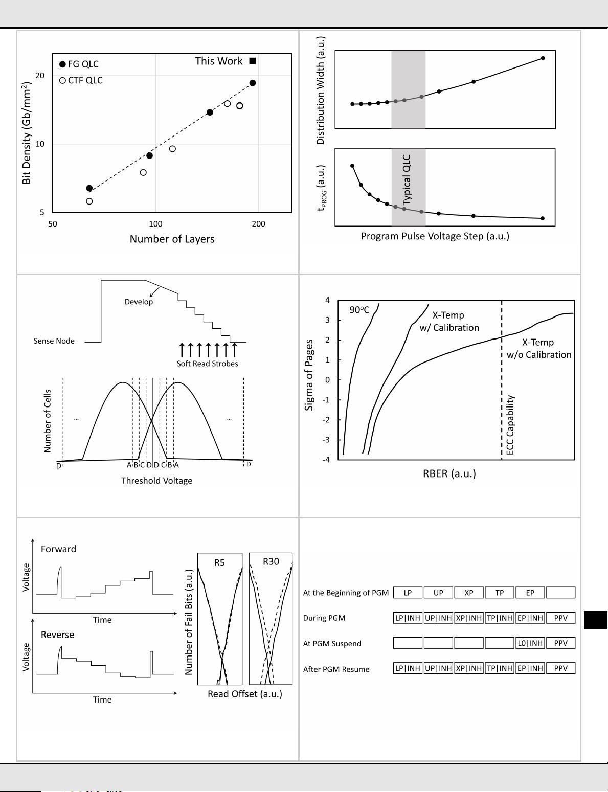
Figure 28.1.1 shows the bit density scaling trend with the number of layers,
demonstrating superior scaling efficiency of this work compared to other QLC
implementations. We describe key innovations to enable reliable PLC operation and the
features implemented to support system-level usage, including a fast soft-bit read
algorithm capable of handling the presence of defective BLs; a fast read-calibration
algorithm, and a reverse-read waveform to improve the read margin, SLC-write-through
and program suspend, as well as a resume algorithm compatible with the above read
operations.
Programming 32 states to encode 5b of data per cell, within a limited threshold voltage
window, poses a significant challenge. To minimize the interference from neighboring
WLs, we use a two-pass coarse/fine programming algorithm. The resilience of floating
gate technology to charge loss, compared to charge-trap Flash technology that suffers
from lateral charge diffusion in the nitride layer, is a key enabler to increasing the number
of bits per cell. However, both technologies are affected by random telegraph noise (RTN)
due to traps in the polysilicon channel and the interfaces, which imposes a lower bound
on how tight the states can be placed. As shown in Fig. 28.1.2, reducing the program
gate step is an efficient way to tighten the threshold voltage distributions for TLC and
QLC at the cost of increased program time; however, it offers diminishing benefits beyond
what is typically used for QLC. Therefore, increasing the error correction code (ECC)
capability is required to reliably read the data. Most QLC implementations have already
increased the number of ECC bytes, compared to their TLC counterparts. However, to
avoid the area penalty we kept the number of ECC bytes unchanged and augmented ECC
correction capabilities with a fast soft-bit read (FSBR) algorithm. To maximize the
information that can be encoded in 2b (for a total of 3b including the hard-bit data), we
implemented a 7-strobe read algorithm, which groups the bits into four buckets from
the strongest to weakest confidence. This is achieved by sensing the cells at different
sense currents instead of different WL voltages, by modulating the voltage applied to
the back of the sensing capacitor after it is discharged in proportion to the BL current,
as shown in Fig. 28.1.3. The average read time (t
R
) for the proposed FSBR is 354s and
a balanced 6-6-7-6-6 Gray code was used to limit the maximum t
R
to 386s.
NAND-Flash memories typically include additional redundant columns to repair defective
BLs. In this work, to further decrease the die area, we reduced the number of redundant
columns by more than 70%, and allow for unrepaired defective BLs, which may be
present in a small percentage of the dies, so long as the unrepaired BLs contribution to
the raw bit error rate (RBER) is significantly smaller than the error correction capability.
However, the presence of unrepaired defective BLs adversely impacts the quality of soft-
read operation since these bits are sensed as the strongest 0s and 1s. To circumvent
this, special open/short sensing operations were added to the read algorithm to identify
defective BLs and place them in the weakest confidence bucket, as shown in Fig. 28.1.3.
With the tight spacing between the threshold voltage states, it is extremely important to
place the read levels at the optimal location between neighboring states. While optimum
read levels are set during NAND manufacturing, die-to-die variations during the lifetime
of the NAND operation and under cross-temperature (x-temp) conditions cannot be fully
compensated. To address this, we implemented a 5-strobe fast read calibration algorithm
by modulating the voltage applied to the back of the sensing capacitor and counting the
number of bits that flip between strobes. Experimental data shows that this scheme is
more accurate than the 3-strobe algorithm proposed earlier [1]. Moreover, compared to
algorithms that are based on counting the total number of bits that belong to different
states [3], the proposed algorithm does not require a perfectly uniform threshold voltage
distribution, which is difficult to achieve with an increased number of states. Figure 28.1.4
reports the RBER distribution; thereby, demonstrating the robustness of the proposed
algorithm to bring the RBER well below the ECC correction capability even under x-temp
conditions.
To further improve the read margin and reduce the RBER, a reverse read waveform is
implemented, as shown schematically in Fig. 28.1.5. Traditionally, the motivation to
implement a reverse read has been to reduce t
R
by avoiding the slow ramp down of the
pass voltage to the lowest read level, which is present in a forward read waveform.
However, in this work the main motivation is to improve the read margin for the higher
read levels with a negligible effect on the lower levels: shown through experimental data
in Fig. 28.1.5. With a forward read waveform, the cells with a higher threshold voltage
are kept in the depletion regime during earlier read levels, with a significantly different
trap occupancy compared to the inversion regime where they are being sensed. The
reverse waveform improves the read margin by maintaining these cells in the inversion
regime prior to their corresponding sense operation.
In order to enable a balanced Gray data encoding, all five pages of data are needed in
both the first and second pass of the program algorithm. While this is the norm for most
QLC implementations except [1], it requires the storage of a few megabytes of data per
die in a DRAM or similar media. Instead, we use a 1b/cell (SLC) cache on the NAND die
to store the data needed for the two-pass PLC programming algorithm. To keep the area
overhead of the SLC cache to less than 2%, we improved the SLC reliability to 250k
program/erase (P/E) cycles, commensurate with 1k of P/E cycle capability in the present
PLC work.
The capability to suspend the program algorithm, to service read requests, is extremely
important for enterprise-level mixed workloads. To minimize the static page buffer (SPB)
area, we did not add extra data latches beyond what is needed for the QLC program
operation and encoded inhibit information during the program algorithm as erase data
(L0). To support FSBR during a program suspend, a minimum of 3 data latches are
needed per BL. To enable this, we rely on the fact that a copy of the data being
programmed is available in the SLC cache. When a program suspend command is
received, the die constructs the inhibit information (INH) by performing a logical AND
operation between the data latches, keeps INH in one of the latches, and releases the
rest of the latches for the read operation. To resume the program operation, the user
data is first read from the SLC cache, combined with the INH information through a
logical OR operation, and then restored to the corresponding data latches, as illustrated
in Fig. 28.1.6.
A die photograph of the fabricated NAND chip is shown in Fig. 28.1.7 along with key
metrics of the present work.
References:
[1] A. Khakifirooz et al., “A 1Tb 4b/Cell 144-Tier Floating-Gate 3D-NAND Flash Memory
with 40MB/s Program Throughput and 13.8Gb/mm
2
Bit Density,” ISSCC, pp. 424-425,
2021.
[2] T. Pekny et al., “A 1-Tb Density 4b/Cell 3D-NAND Flash on 176-Tier Technology with
4-Independent Planes for Read Using CMOS-Under-the-Array,” ISSCC, pp. 132-133,
2022.
[3] W. Cho et al., “A 1-Tb, 4b/cell, 176-stacked-WL 3D-NAND Flash Memory with
Improved Read Latency and a 14.8Gb/mm
2
Density,” ISSCC, pp. 134-135, 2022.
[4] J. Yuh et al., “A 1-Tb 4b/Cell 4-Plane 162-Layer 3D Flash Memory with a 2.4-Gb/s
I/O Speed Interface,” ISSCC, pp. 130-131, 2022.
[5] M. Kim et al., “A 1Tb 3b/Cell 8th-Generation 3D-NAND Flash Memory with 164MB/s
Write Throughput and a 2.4Gb/s Interface,” ISSCC, pp. 136-137, 2022.
978-1-6654-9016-0/23/$31.00 ©2023 IEEE

401
ISSCC 2023 / February 22, 2023 / 8:30 AM
DIGEST OF TECHNICAL PAPERS •
Figure 28.1.1: Bit density comparison of the proposed PLC die vs prior QLC
implementations in floating-gate (FG) and charge-trap Flash technologies.
Figure 28.1.2: Average threshold voltage distribution width and the 2
nd
pass program
time as a function of the program gate step. Plots show the diminishing benefit of
reducing the gate steps in tightening the distributions.
Figure 28.1.3: The FSBR algorithm uses boost modulation to group the bits into four
buckets from highest (A) to lowest (D) confidence. Defective (open/short) BLs are
placed in the lowest confidence bucket.
Figure 28.1.4: RBER distribution under cross-temperature condition, demonstrating
the strength of the proposed fast-read calibration algorithm to lower the RBER well
below the ECC correction capability.
Figure 28.1.5: Schematic illustration of the forward and reverse read waveforms and
representative experimental data, which demonstrates an improved read margin for
higher read levels with reverse read (solid line: RR, dashed line: FR).
Figure 28.1.6: SPB latch allocation for user data, inhibit, and pre-program verify
(PPV) information, to support FSBR during program suspend.
28
剩余25页未读,继续阅读
资源评论

LittleBrightness
- 粉丝: 0
- 资源: 147
上传资源 快速赚钱
 我的内容管理
展开
 我的资源
快来上传第一个资源
 我的收益 登录查看自己的收益
 我的积分
登录查看自己的积分
 我的C币
登录后查看C币余额
 我的收藏
我的收藏  我的下载
我的下载  下载帮助
下载帮助

 前往需求广场,查看用户热搜
最新资源
资源上传下载、课程学习等过程中有任何疑问或建议,欢迎提出宝贵意见哦~我们会及时处理!
点击此处反馈


安全验证
文档复制为VIP权益,开通VIP直接复制
 信息提交成功