


© Copyright ARM Limited 2009. All rights reserved.
Low Pin-count Debug Interfaces for
Multi-device Systems
Michael Williams
*
ARM Limited, 110 Fulbourn Road, Cambridge, England.
*
michael.williams@arm.com
Abstract-IEEE Std 1149.1-2001 Standard Test Access Port and
Boundary-Scan Architecture (JTAG) is widely used as a debug
interface, providing a path for a debugger to access debug com-
ponents in complex systems-on-chip (SoCs). By its very nature
JTAG accommodates systems containing multiple devices. How-
ever, JTAG was primarily intended as a component and board
test interface, and is not ideally suited as a debug interface. Its
shortcomings have led the industry to search for an alternative.
As a result, JTAG interfaces have started to be displaced by
dedicated debug interfaces. This paper examines some of these
alternatives, and concludes that a dedicated serial wire debug
interface can be delivered with lower pin-count and higher per-
formance, whilst maintaining support for multi-device systems
and interoperability with test.
I. INTRODUCTION
JTAG [1] was originally designed and intended as a test in-
terface. The four- or five-pin interface comprises two unidi-
rectional data pins (TDI and TDO), a clock (TCK), state
machine control pin (TMS) and optional reset (TRST#). This
use of unidirectional data pins at either end of a scan-chain
connected to the registers being accessed, coupled with a
simple control state-machine allows daisy-chaining of multi-
ple JTAG devices (Fig. 1).
That JTAG is primarily meant for test is reflected in the
specification; for example, the specification requires that each
device implements a single test access port (TAP), and de-
scribes in detail control instructions (INTEST, EXTEST,
SAMPLE, PRELOAD) and scan-chain structures for imple-
menting boundary-scan testing.
JTAG is also widely used as an interface for controlling the
embedded debug features of processors and SoCs. The sim-
plicity and ubiquity of the interface, and its support for con-
necting multiple devices through daisy-chaining made it an
ideal candidate for the first generations of embedded debug.
However, it has several shortcomings, for example:
— JTAG does not make efficient use of the four pins dedi-
cated to it, for example an efficient direct memory access
TAP may only achieve a data rate of 640Kbytes/sec per
data pin at 20MHz;
— using JTAG to access multiple debug components on a
single SoC (as in Fig. 1) is not strictly allowed by the
standard;
— daisy-chaining is intolerant to a debug component and its
TAP being removed from the system, for example as a
result of power management.
Recent developments in debug interface technology have
attempted to address some of these concerns. The primary
focus has been on reducing pin-count.
II. LOW PIN-COUNT INTERFACES
An alternative to JTAG for debug should fulfil the follow-
ing requirements:
— maximum of two pins: vital for very low connectivity
devices or packages;
— support for multiple devices connected simultaneously;
— inter-operability with other debug and test interfaces;
— allow debug through legacy JTAG TAP controllers;
— high performance data rates;
— synthesis-friendly with high maximum clock rate;
— low power;
— small silicon area;
— low tools costs;
— reliable in the face of errors and safe from glitches on
pins when tools not connected.
This paper outlines three approaches to a low pin-count in-
terface, describing the third, preferred approach in more de-
tail:
— time-division multiplexed JTAG interface;
— re-visiting the JTAG standard (IEEE 1149.7);
— dedicated serial wire debug interface.
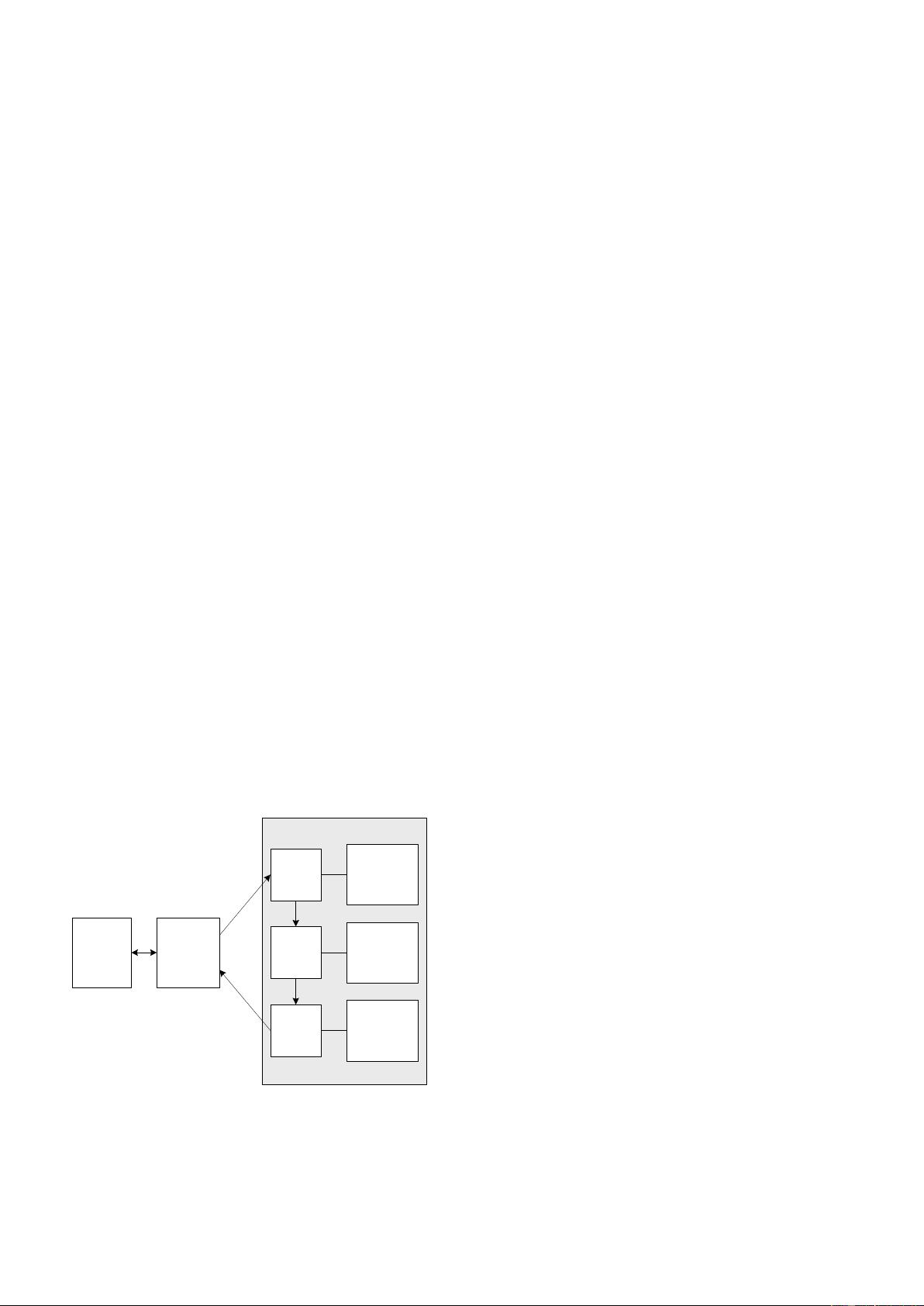
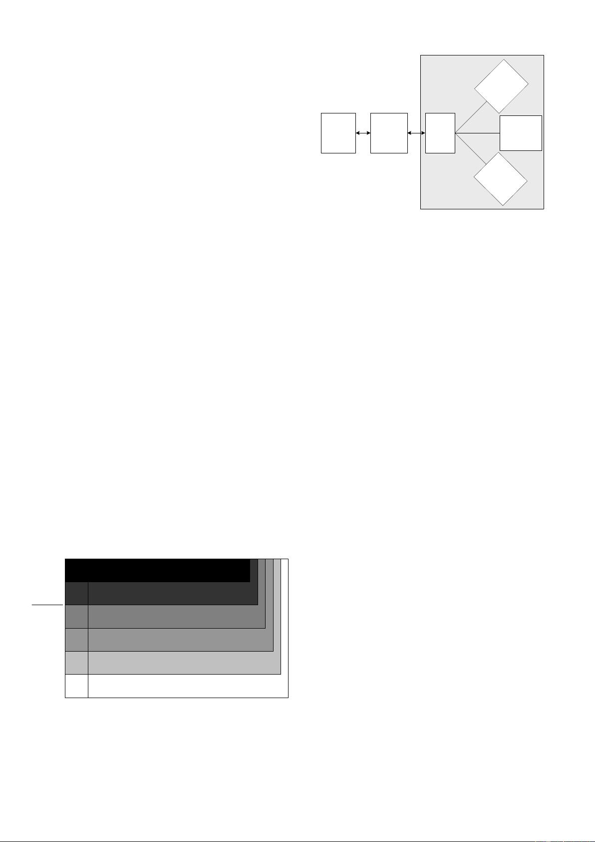
System-on-Chip
Host
controller
Debug
component
2
Access
Port 1
Protocol
converter
Access
Port 3
Debug
component
1
Debug
component
3
Access
Port 2
Fig. 1: Daisy-chain debug topology


评论0