没有合适的资源?快使用搜索试试~ 我知道了~
Class-E类功率放大器的波形推导原始论文
需积分: 0 10 下载量 48 浏览量
2023-02-25
10:28:31
上传
评论
收藏 1008KB PDF 举报
温馨提示
试读
11页
Class-E类功率放大器的波形推导原始论文 在高自由状态下的E类波形应该是怎么样的呢,其实在60年前就有学者给出了计算的的公式(Idealized operation of the class_E tuned power amplifier),但是其计算比较复杂且涉及各种方程的求解,在此我对其进行了分析,并写成了Matlab代码的形式,大家只需要修改占空比参数和导数条件参数即可得到波形,为自己的分析助力。 原文链接:https://blog.csdn.net/weixin_44584198/article/details/129212457
资源推荐
资源详情
资源评论
IEEE TRANSAClTONS ON CIRCUITS AND SYSTEMS, VOL.
CAS-24,
NO.
12,
DECEMBER
1977
725
Idealized Operation of the Class E Tuned
Power Amplifier
FREDERICK H. RAAB,
MEMBER, IEEE
Absfracr-The class E tuned power amplifier consists of a load network
and a single transistor that is operated as a switch at tbe carrier frequency
of tbe output signal. ‘zbe most simple type of load network consists of a
capacitor shunting tbe transistor and a series-tuned output circuit, which
may bave a residual reactance. Circuit operation is determined by tbe
transistor when it is on, and by the transient response of the load network
when tbe transistor is off. The basic equations governing amplifier opera-
tion are derived using Fourier series techniques and a high-Q assumption.
These equations are then used to determine component values for opti-
mum operation at an efficiency of 100 percent. Other combinations of
component values and duty cycles which result in lOO-percent efficiency
are also determined. ‘fbe barmouic structure of tbe collector voltage
waveform is analyzed and related amplifier configurations are discussed.
While tbis analysis is directed toward the design of bigbefficiency power
amplifiers, it also provides insight into tbe operation of modern solid-state
VHF-UHF tuned power amplifiers.
I.
INTRODUCTION
T
HE “class E” concept recently introduced by the
Sokals [l], [2] offers a new means of highly efficient
power amplification. This paper expands upon the Sokals’
work by providing an analytical basis for class E opera-
tion and by deriving additional amplifier configurations.
Before entering the technical discussion, some definitions
must be clarified.
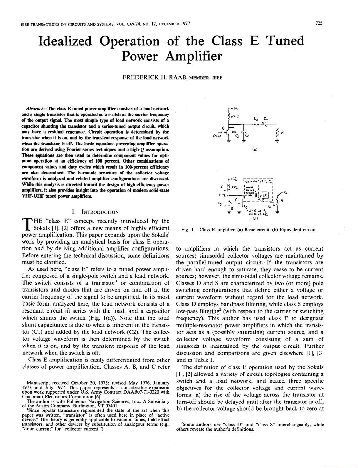
As used here, “class E” refers to a tuned power ampli-
fier composed of a single-pole switch and a load network.
The switch consists of a transistor’ or combination of
transistors and diodes that are driven ‘on and off at the
carrier frequency of the signal to be amplified. In its most
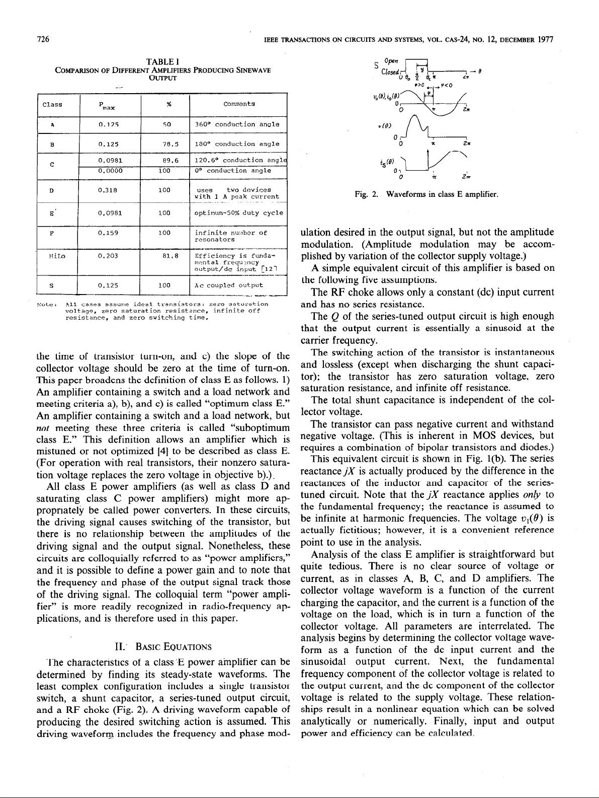
basic form, analyzed here, the load network consists of a
resonant circuit iii series with the load, and a capacitor
which shunts the switch (Fig. l(a)). Note that the total
shunt capacitance is due to what is inherent in the transis-
tor (Cl) and added by the load network (C2). The collec-
tor voltage waveform is then determined by the switch
when it is on, and by the transient response of the load
network when the switch is off.
Class E amplification is easily differentiated from other
classes of power amplification. Classes A, B, and C refer
Manuscript received October 30, 1975; revised May 1976, January
1977, and July 1977. This paper represents a considerable expansion
upon work supported under U.S. Army Contract DAAB07-71-0220 with
Cincinnati Electronics Corporation [6].
The author is with Polhemus Navigation Sciences, Inc., A Subsidiary
of the Austin Company, Burlington, VT 05401.
‘Since bipolar transistors represented the state of the art when this
paper was written,
“transistor” is often used here in place of “active
device.” The theory is generally applicable to vacuum tubes, field-effect
transistors, and other devices by substitution of analogous terms (e.g.,
“drain current” for “collector current.“)
R
(b)
Fig. 1. Class E amplifier. (a) Basic circuit. (b) Equivalent circuit.
to amplifiers in which the transistors act as current
sources; sinusoidal collector voltages are maintained by
the parallel-tuned output circuit. If the transistors are
driven hard enough to saturate, they cease to be current
sources; however, the sinusoidal collector voltage remains.
Classes D and S are characterized by two (or more) pole
switching configurations that define either a voltage or
current waveform without regard for the load network.
Class D employs bandpass filtering, while class S employs
low-pass filtering2 (with respect to the carrier or switching
frequency). This author has used class F to designate
multiple-resonator power amplifiers in which the transis-
tor acts as a (possibly saturating) current source, and a
collector voltage waveform consisting of a sum of
sinusoids is maintained by the output circuit. Further
discussion and comparisons are given elsewhere [l], [3]
and in Table I.
The definition of class E operation used by the Sokals
[l], [2] allowed a variety of circuit topologies containing a
switch and a load network, and stated three specific
objectives for the collector voltage and current wave-
forms: a) the rise of the voltage across the transistor at
turn-off should be delayed until after the transistor is off,
b) the collector voltage should be brought back to zero at
*Some authors use “class D” and “class s” interchangeably, while
others reverse the author’s definitions.
Authorized licensed use limited to: University of Electronic Science and Tech of China. Downloaded on June 22,2022 at 06:00:57 UTC from IEEE Xplore. Restrictions apply.
726
IEEE TRANSACTIONS ON CIRCUITS AND SYSTEMS, VOL. CAS-24, NO. 12. DECEMBER 1977
TABLE I
COMPARISON OF DIFFERENT AMPLIFIERS PRODUCING SINEWAVE
OUTFUT
two devices
nfinite nu:?ber of
!$ote :
411 cases assume ideal transistors: zero saturation
v01tag4,
zero saturation resistance. infinite off
resistance. and zero switching
time.
the time of transistor turn-on, and c) the slope of the
collector voltage should be zero at the time of turn-on.
This paper broadens the definition of class E as follows. 1)
An amplifier containing a switch and a load network and
meeting criteria a), b), and c) is called “optimum class E.”
An amplifier containing a switch and a load network, but
not meeting these three criteria is called “suboptimum
class E.” This definition allows an amplifier which is
mistuned or not optimized [4] to be described as class E.
(For operation with real transistors, their nonzero satura-
tion voltage replaces the zero voltage in objective b).).
All class E power amplifiers (as well as class D and
saturating class C power amplifiers) might more ap-
propriately be called power converters. In these circuits,
the driving signal causes switching of the transistor, but
there is no relationship between the amplitudes of the
driving signal and the output signal. Nonetheless, these
circuits are colloquially referred to as “power amplifiers,”
and it is possible to define a power gain and to note that
the frequency and phase of the output signal track those
of the driving signal. The colloquial term “power ampli-
fier” is more readily recognized in radio-frequency ap-
plications, and is therefore used in this paper.
11:
BASIC
EQUATIONS
The characteristics of a class .E power amplifier can be
determined by finding its steady-state waveforms. The
least complex configuration includes a single transistor
switch, a shunt capacitor, a series-tuned output circuit,
and a RF choke (Fig. 2). A driving waveform capable of
producing the desired switching action is assumed. This
driving waveform includes the frequency and phase mod-
1
in
% (;;p
is@Joy+
b i Zn
Fig. 2.
Waveforms in class E amplifier.
ulation desired in the output signal, but not the amplitude
modulation. (Amplitude modulation may be accom-
plished by variation of the collector supply voltage.)
A simple equivalent circuit of this amplifier is based on
the following five assumptions.
The RF choke allows only a constant (dc) input current
and has no series resistance.
The Q of the series-tuned output circuit is high enough
that the output current is essentially a sinusoid at the
carrier frequency.
The switching action of the transistor is instantaneous
and lossless (except when discharging the shunt capaci-
tor); the transistor has zero saturation voltage, zero
saturation resistance, and infinite off resistance.
The total shunt capacitance is independent of the col-
lector voltage.
The transistor can pass negative current and withstand
negative voltage. (This is inherent in MOS devices, but
requires a combination of bipolar transistors and diodes.)
This equivalent circuit is shown in Fig. l(b). The series
reactance jX is actually produced by the difference in the
reactances of the inductor and capacitor of the series-
tuned circuit. Note that thejX reactance applies on& to
the fundamental frequency; the reactance is assumed to
be infinite at harmonic frequencies. The voltage u,(e) is
actually fictitious; however, it is a convenient reference
point to use in the analysis.
Analysis of the class E amplifier is straightforward but
quite tedious. There is no clear source of voltage or
current, as in classes A, B, C, and D amplifiers. The
collector voltage waveform is a function of the current
charging the capacitor, and the current is a function of the
voltage on the load, which is in turn a function of the
collector voltage. All parameters are interrelated. The
analysis begins by determining the collector voltage wave-
form as a function of the dc input current and the
sinusoidal output current. Next, the fundamental
frequency component of the collector voltage is related to
the output current;and the dc component of the collector
voltage is related to the supply voltage. These relation-
ships result in a nonlinear equation which can be solved
analytically or numerically. Finally, input and output
power and efficiency can be calculated.
Authorized licensed use limited to: University of Electronic Science and Tech of China. Downloaded on June 22,2022 at 06:00:57 UTC from IEEE Xplore. Restrictions apply.
RAAB: OPERATION OF CLASS E TUNED PA
727
A. Basic Relationships
The output voltage and current are sinusoidal and have
the forms
u,(~)=c sin (wt+cp)=c sin (0+cp)
(2.1)
and
iO(f3)= $
sin (e+cp)
(2.2)
where 0 is an “angular time” used for mathematical
convenience. The parameters c and rp are to be de-
termined; cp is defined in Fig. 2.
The hypothetical voltage u,(0) is also a sinusoid, but
has a different phase because of reactance X
u1(e)=%(e)+%(e)
(2.3)
=C
sin
(e+q)+x$ cos (e+cp)
(2.4)
=c, sin
(e+q,)
(2.5)
where
c,=c
i
1,s =pc
and
Since the RF choke forces a dc input current and the
series-tuned output circuit forces a sinusoidal output cur-
rent, the difference between those two currents must flow
into (or out of) the switch-capacitor combination. When
switch S is open, the difference flows into capacitor C;
when switch S is closed, the current difference flows
through switch S. If a capacitor voltage of other than zero
volts is present at the time the switch closes, the switch
discharges that voltage to zero volts, dissipating the stored
energy of $ CV2.
For purposes of this analysis, the discharge of the
capacitor may be assumed to be a current impulse
qS (0 -
e,), where 0, is the time at which the switch closes.
However, in a real amplifier, discharge of the capacitor
requires a nonzero length of time, during which the collec-
tor voltage and current are simultaneously nonzero. In
any case, however, the total dissipation is the energy
stored in the capacitor, and does not depend on the
particulars of the discharge waveforms. The model re-
mains valid as long as the time required to discharge the
capacitor is a relatively small fraction of the RF cycle.
When S is off, the collector voltage is produced by the
charging of capacitor C by the difference current, hence,
where 0, indicates the time at which S opens.
Since the nonzero collector voltage appears when the
transistor is off, it is convenient to describe the waveforms
in terms of the half off-time y, which is in radians. The
center of the off-time is arbitrarily defined as 7r/2 (Fig. 2).
The switching instants are now 0, = a/2-y and 0, = 7r/2
+y. Note that in the event that 0, < 0 and is therefore
outside of the 277 interval corresponding to one cycle, it
can be repaced by &,+27, with appropriate modification
to the integral in (2.8). Equivalently, the interval of a cycle
can be redefined when necessary. The collector voltage at
time 0 can now be evaluated by expanding (2.8)
(2.9)
+$e+&
cOs(e+cp)
where
B=wC.
(2.11)
Since the tuned circuit has zero impedance to funda-
mental frequency current, there can be no fundamental
frequency voltage drop across it. This means that the
fundamental frequency component of the collector volt-
age waveform must be the hypothetical voltage u,(B). The
magnitude of this component can be calculated by a
Fourier integral. Unfortunately, the collector voltage is
not symmetrical around 7r/2, which makes the phase cp an
unknown.
B. Fourier Analysis
The magnitude c, of the fundamental frequency compo-
nent of the collector voltage is then
c,= -
~]02”o(e)
sin
(e+cpl)
dB
(2.12)
=
4 -$(t-Y+‘P~)+--$
My-d]
.coscp, siny+$
[
-2 sin ‘pi siny
-&[sin(2’p+$) sin2y-2y sin$]. (2.13)
It is now possible to solve for c by substituting pc for c,
and collecting terms
pc+c
sin (2~ + Ir/) sin 2y - 2y sin I+L
2rBR
+
2 sin (y - cp) cos cpr sin y
?TBR
1
=$c-
77+2y-29,+7r+2r+7,) cos cp, siny
+(2y cosy-2 siny) sinq,]. (2.14)
Authorized licensed use limited to: University of Electronic Science and Tech of China. Downloaded on June 22,2022 at 06:00:57 UTC from IEEE Xplore. Restrictions apply.
剩余10页未读,继续阅读
资源评论
怡步晓心l
- 粉丝: 8388
- 资源: 97
上传资源 快速赚钱
- 我的内容管理 展开
- 我的资源 快来上传第一个资源
- 我的收益 登录查看自己的收益
- 我的积分 登录查看自己的积分
- 我的C币 登录后查看C币余额
- 我的收藏
- 我的下载
- 下载帮助
最新资源
- Pytorch-pytorch深度学习教程之深度残差网络.zip
- Pytorch-pytorch深度学习教程之循环神经网络.zip
- Pytorch-pytorch深度学习教程之逻辑回归.zip
- Pytorch-pytorch深度学习教程之双向循环网络.zip
- Pytorch-pytorch深度学习教程之卷积神经网络.zip
- Pytorch-pytorch深度学习教程之前馈神经网络.zip
- Pytorch-pytorch深度学习教程之线性回归.zip
- Pytorch-pytorch深度学习教程之基本操作.zip
- 基于QT的地图可视化桌面系统后台数据库为MySQL5.7源码.zip
- 基于simulink的PLL锁相环系统仿真【包括模型,文档,参考文献,操作步骤】
资源上传下载、课程学习等过程中有任何疑问或建议,欢迎提出宝贵意见哦~我们会及时处理!
点击此处反馈
安全验证
文档复制为VIP权益,开通VIP直接复制
信息提交成功