没有合适的资源?快使用搜索试试~ 我知道了~
TI的TLV320AIC33规格书
需积分: 5 0 下载量 175 浏览量
2022-12-02
15:51:02
上传
评论
收藏 1.69MB PDF 举报
温馨提示
试读
93页
TI的TLV320AIC33规格书
资源推荐
资源详情
资源评论
1
FEATURES
DESCRIPTION
TLV320AIC33
www.ti.com
........................................................................................................................................... SLAS480B – JANUARY 2006 – REVISED DECEMBER 2008
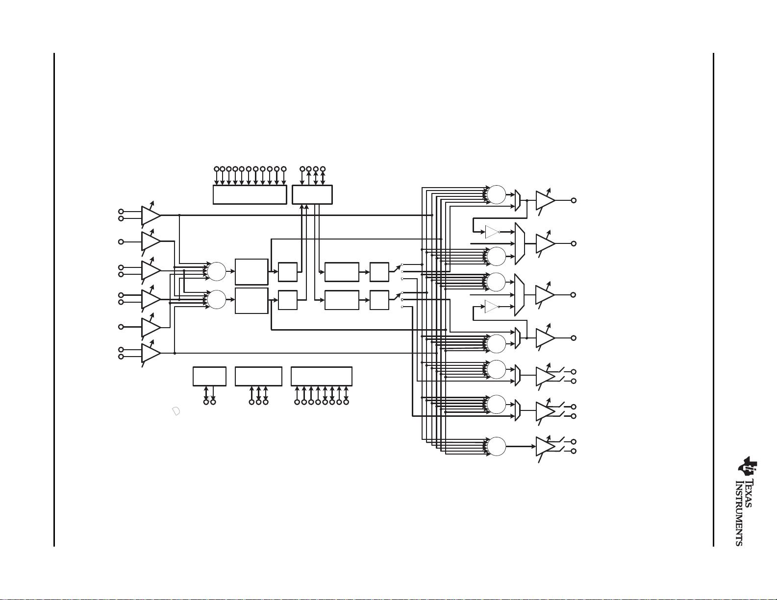
Low Power Stereo Audio CODEC for Portable Audio/Telephony
7 × 7 mm 48-QFN
23
• Stereo Audio DAC
– 100-dBA Signal-to-Noise Ratio
The TLV320AIC33 is a low power stereo audio codec
– 16/20/24/32-Bit Data
with stereo headphone amplifier, as well as multiple
– Supports Rates From 8 kHz to 96 kHz
inputs and outputs programmable in single-ended or
– 3D/Bass/Treble/EQ/De-emphasis Effects
fully differential configurations. Extensive register-
based power control is included, enabling stereo
• Stereo Audio ADC
48-kHz DAC playback as low as 14 mW from a 3.3-V
– 92-dBA Signal-to-Noise Ratio
analog supply, making it ideal for portable
– Supports Rates From 8 kHz to 96 kHz
battery-powered audio and telephony applications.
• Ten Audio Input Pins
The record path of the TLV320AIC33 contains
– Programmable in Single-Ended or Fully
integrated microphone bias, digitally controlled stereo
Differential Configurations
microphone preamplifier, and automatic gain control
(AGC), with mix/mux capability among the multiple
– 3-State Capability for Floating Input
analog inputs. The playback path includes mix/mux
Configurations
capability from the stereo DAC and selected inputs,
• Seven Audio Output Drivers
through programmable volume controls, to the
– Stereo 8- Ω , 500-mW/Channel Speaker Drive
various outputs.
Capability
The TLV320AIC33 contains four high-power output
– Stereo Fully Differential or Single-Ended
drivers as well as three fully differential output drivers.
Headphone Drivers
The high-power output drivers are capable of driving
a variety of load configurations, including up to four
– Fully Differential Stereo Line Outputs
channels of single-ended 16- Ω headphones using
– Fully Differential Mono Output
ac-coupling capacitors, or stereo 16- Ω headphones in
• Low Power: 14-mW Stereo 48-kHz Playback
a capacitorless output configuration. In addition, pairs
With 3.3-V Analog Supply
of drivers can be used to drive 8- Ω speakers in a BTL
configuration at 500 mW per channel.
• Programmable Input/Output Analog Gains
• Automatic Gain Control (AGC) for Record
The stereo audio DAC supports sampling rates from
8 kHz to 96 kHz and includes programmable digital
• Programmable Microphone Bias Level
filtering in the DAC path for 3D, bass, treble,
• Programmable PLL for Flexible Clock
midrange effects, speaker equalization, and
Generation
de-emphasis for 32-kHz, 44.1-kHz, and 48-kHz rates.
• Control Bus Selectable SPI or I
2
C
The stereo audio ADC supports sampling rates from
8 kHz to 96 kHz and is preceded by programmable
• Audio Serial Data Bus Supports I
2
S,
gain amplifiers providing up to +59.5-dB analog gain
Left/Right-Justified, DSP, and TDM Modes
for low-level microphone inputs.
• Alternate Serial PCM/I
2
S Data Bus for Easy
The serial control bus supports SPI or I
2
C protocols,
Connection to Bluetooth™ Module
while the serial audio data bus is programmable for
• Digital Microphone Input Support
I
2
S, left/right-justified, DSP, or TDM modes. A highly
• Extensive Modular Power Control
programmable PLL is included for flexible clock
generation and support for all standard audio rates
• Power Supplies:
from a wide range of available MCLKs, varying from
– Analog: 2.7 V – 3.6 V.
512 kHz to 50 MHz, with special attention paid to the
– Digital Core: 1.65 V – 1.95 V
most popular cases of 12-MHz, 13-MHz, 16-MHz,
19.2-MHz, and 19.68-MHz system clocks.
– Digital I/O: 1.1 V – 3.6 V
• Packages: 5 × 5 mm 80-VFBGA;
1
Please be aware that an important notice concerning availability, standard warranty, and use in critical applications of Texas
Instruments semiconductor products and disclaimers thereto appears at the end of this data sheet.
2 MIcroStar Junior is a trademark of Texas Instruments.
3 Bluetooth is a trademark of Bluetooth SIG, Inc..
PRODUCTION DATA information is current as of publication date.
Copyright © 2006 – 2008, Texas Instruments Incorporated
Products conform to specifications per the terms of the Texas
Instruments standard warranty. Production processing does not
necessarily include testing of all parameters.
DESCRIPTION (CONTINUED)
SIMPLIFIED BLOCK DIAGRAM
LINE_OUT_L+
LINE_OUT_L−
LINE_OUT_R+
LINE_OUT_R−
MONO_OUT+
MONO_OUT
−
HPR+
HPL−/HPLCOM
HPL+
MIC2/LINE2L+
MIC2/LINE2L−
MIC1/LINE1L+
MIC1/LINE1L−
MIC1/LINE1R+
MIC1/LINE1R−
MIC3/LINE3R
MIC3/LINE3L
PGA
0/+59.5dB
0.5dB
steps
ADC
ADC
AudioSerial
Bus
DAC
L
DAC
R
DIN
DOUT
BCLK
WCLK
SPI/I2CSerialControl
Bus
SELECT
CSEL/I2C_ADR0
SCLK/I2C_ADR1
MOSI/GPIO
MISO/GPIO
AudioClock
Generation
MCLK
GPIO_1
GPIO_2
Bias/
Reference
MICBIAS
VoltageSupplies
AVDD_DAC
AVSS_DAC
DRVDD
DRVSS
DVDD
DVSS
IOVDD
VolumeCtl
&Effects
VolumeCtl
&Effects
DRVDD
DRVSS
SCL/GPIO
SDA/GPIO
AVDD_ADC
AVSS_ADC
RESETB
MICDET
MIC2/LINE2R−
MIC2/LINE2R+
+
+
VCM
+
+
+
HPR−/HPRCOM/
SPKFC
+
VCM
+
PGA
0/+59.5dB
0.5dB
steps
+
+
TLV320AIC33
SLAS480B – JANUARY 2006 – REVISED DECEMBER 2008 ...........................................................................................................................................
www.ti.com
The TLV320AIC33 operates from an analog supply of 2.7 V – 3.6 V, a digital core supply of 1.65 V – 1.95 V, and a
digital I/O supply of 1.1 V – 3.6 V. The device is available in 5 × 5-mm, 80-ball MIcroStar Junior™ BGA and
7 × 7-mm, 48-lead QFN.
2 Submit Documentation Feedback Copyright © 2006 – 2008, Texas Instruments Incorporated
Product Folder Link(s): TLV320AIC33
PIN ASSIGNMENTS
A
1 2 3 4
5
6
7
8 9
B
C
D
E
F
G
H
J
48−leadQFNPackage(Bottomview) 5x5mm80−BallBGA Package(BottomView)
48
1
12
13
24
25
36
37
(Nottoscale) =NC
TLV320AIC33
www.ti.com
........................................................................................................................................... SLAS480B – JANUARY 2006 – REVISED DECEMBER 2008
PACKAGING/ORDERING INFORMATION
PACKAGE OPERATING ORDERING TRANSPORT
PRODUCT PACKAGE DESIGNATOR TEMPERATURE NUMBER MEDIA, QUANTITY
RANGE
TLV320AIC33IZQE Trays, 360
ZQE
TLV320AIC33IZQER Tape and Reel, 3000
BGA-80
TLV320AIC33IGQE Trays, 360
TLV320AIC33 GQE – 40 ° C to 85 ° C
TLV320AIC33IGQER Tape and Reel, 3000
TLV320AIC33IRGZT Tape and Reel, 250
QFN-48 RGZ
TLV320AIC33IRGZR Tape and Reel, 2000
Connect QFN thermal pad to DRVSS.
The shaded balls on BGA package are not connected to the die, but are electrically connected to each other.
TERMINAL FUNCTIONS
TERMINAL
DESCRIPTION
BGA
QFN NAME
BALL
A2 13 MICBIAS Microphone Bias Voltage Output
A1 14 MIC3R MIC3 Input (Right or Multifunction)
C2,D2 15 AVSS_ADC Analog ADC Ground Supply, 0 V
B1,C1 16,17 DRVDD ADC Analog and Output Driver Voltage Supply, 2.7 V – 3.6 V
D1 18 HPLOUT High-Power Output Driver (Left Plus)
E1 19 HPLCOM High-Power Output Driver (Left Minus or Multifunctional)
E2,F2 20,21 DRVSS Analog Output Driver Ground Supply, 0 V
F1 22 HPRCOM High-Power Output Driver (Right Minus or Multifunctional)
G1 23 HPROUT High-Power Output Driver (Right Plus)
H1 24 DRVDD ADC Analog and Output Driver Voltage Supply, 2.7 V – 3.6 V
Copyright © 2006 – 2008, Texas Instruments Incorporated Submit Documentation Feedback 3
Product Folder Link(s): TLV320AIC33
TLV320AIC33
SLAS480B – JANUARY 2006 – REVISED DECEMBER 2008 ...........................................................................................................................................
www.ti.com
TERMINAL FUNCTIONS (continued)
TERMINAL
DESCRIPTION
BGA
QFN NAME
BALL
J1 25 AVDD Analog DAC Voltage Supply, 2.7 V – 3.6 V
G2,H2 26 AVSS_DAC Analog DAC Ground Supply, 0 V
J2 27 MONO_LOP Mono Line Output (Plus)
J3 28 MONO_LOM Mono Line Output (Minus)
J4 29 LEFT_LOP Left Line Output (Plus)
J5 30 LEFT_LOM Left Line Output (Minus)
J6 31 RIGHT_LOP Right Line Output (Plus)
J7 32 RIGHT_LOM Right Line Output (Minus)t
H8 33 RESET Reset
General-Purpose Input/Output #2 (Input/Output) / Digital Microphone Data Input / PLL Clock Input /
J8 34 GPIO2
Audio Serial Data Bus Bit Clock Input/Output
General-Purpose Input/Output #1 (Input/Output) / PLL/Clock Mux Output / Short Circuit Interrupt /
J9 35 GPIO1
AGC Noise Flag / Digital Microphone Clock Audio Serial Data Bus Word Clock Input/Output
H9 36 DVDD Digital Core Voltage Supply, 1.65V – 1.95V
G8 37 MCLK Master Clock Inputt
G9 38 BCLK Audio Serial Data Bus Bit Clock (Input/Output)
F9 39 WCLK Audio Serial Data Bus Word Clock (Input/Output)
E9 40 DIN Audio Serial Data Bus Data Input (Input)
F8 41 DOUT Audio Serial Data Bus Data Output (Output)t
D9 42 DVSS Digital Core / I/O Ground Supply, 0V
E8 43 SELECT Control Mode Select Pin (1=SPI, 0=I
2
C)
C9 44 IOVDD I/O Voltage Supply, 1.1V – 3.6V
B8 45 MFP0 Multifunction pin #0 - SPI Chip Select / GPI / I
2
C Address Pin #0
B9 46 MFP1 Multifunction pin #1 - SPI Serial Clock / GPI / I
2
C Address Pin #1S
A8 47 MFP2 Multifunction pin #2 - SPI MISO Slave Serial Data Output / GPOI
A9 48 MFP3 Multifunction pin #3 - SPI MOSI Slave Serial Data Input / GPI / Audio Serial Data Bus Data Input
C8 1 SCL I
2
C Serial Clock / GPIO
D8 2 SDA I
2
C Serial Data Input/Output / GPIO
A7 – NC No Connect
A6 3 LINE1LP MIC1 or Line1 Analog Input (Left Plus or Multifunction)
A5 4 LINE1LM MIC1 or Line1 Analog Input (Left Minus or Multifunction)
B7 5 LINE1RP MIC1 or Line1 Analog Input (Right Plus or Multifunction)
B6 6 LINE1RM MIC1 or Line1 Analog Input (Right Minus or Multifunction)
A4 7 LINE2LP MIC2 or Line2 Analog Input (Left Plus or Multifunction)
B5 8 LINE2LM MIC2 or Line2 Analog Input (Left Minus or Multifunction)
B4 9 LINE2RP MIC2 or Line2 Analog Input (Right Plus or Multifunction)
A3 10 LINE2RM MIC2 or Line2 Analog Input (Right Minus or Multifunction)
B3 11 MIC3L MIC3 Input (Left or Multifunction)
B2 12 MICDET Microphone Detect
C4-C7,
D3-D7,
E3-E7,
– NC Do not connect.
F3-F7,
G3-G7,
H3-H7
4 Submit Documentation Feedback Copyright © 2006 – 2008, Texas Instruments Incorporated
Product Folder Link(s): TLV320AIC33
ABSOLUTE MAXIMUM RATINGS
DISSIPATION RATINGS
(1)
RECOMMENDED OPERATING CONDITIONS
TLV320AIC33
www.ti.com
........................................................................................................................................... SLAS480B – JANUARY 2006 – REVISED DECEMBER 2008
over operating free-air temperature range (unless otherwise noted)
(1) (2)
VALUE UNIT
AVDD to AVSS, DRVDD to DRVSS – 0.3 to 3.9 V
AVDD to DRVSS – 0.3 to 3.9 V
IOVDD to DVSS – 0.3 to 3.9 V
DVDD to DVSS – 0.3 to 2.5 V
AVDD to DRVDD – 0.1 to 0.1 V
Digital input voltage to DVSS – 0.3 V to IOVDD+0.3 V
Analog input voltage to AVSS – 0.3 V to AVDD+0.3 V
Operating temperature range -40 to +85 ° C
Storage temperature range -65 to +105 ° C
T
J
Max Junction temperature 105 ° C
Power dissipation (T
J
Max – T
A
) / θ
JA
θ
JA
Thermal impedance , BGA package 63 ° C/W
Thermal impedance, QFN package 38.5 ° C/W
(1) Stresses beyond those listed under absolute maximum ratings may cause permanent damage to the device. These are stress ratings
only, and functional operation of the device at these or any other conditions beyond those indicated under recommended operating
conditions is not implied. Exposure to absolute-maximum-rated conditions for extended periods may affect device reliability.
(2) ESD complicance tested to EIA / JESD22-A114-B and passed.
T
A
= 25 ° C T
A
= 75 ° C T
A
= 85 ° C
PACKAGE TYPE DERATING FACTOR
POWER RATING POWER RATING POWER RATING
BGA 1.27 W 15.9 mW/ ° C 476 mW 317 mW
QFN 2.08 W 26.0 mW/ ° C 779 mW 519 mW
(1) This data was taken using 2 oz. trace and copper pad that is soldered directly to a JEDEC standard 4-layer 3 in × 3 in PCB.
over operating free-air temperature range (unless otherwise noted)
MIN NOM MAX UNIT
AVDD, Analog supply voltage 2.7 3.3 3.6 V
DRVDD1
/2
(1)
DVDD
(1)
Digital core supply voltage 1.65 1.8 1.95 V
IOVDD
(1)
Digital I/O supply voltage 1.1 1.8 3.6 V
V
I
Analog full-scale 0 dB input voltage (DRVDD1 = 3.3 V) 0.707 V
RMS
Stereo line-output load resistance 10 k Ω
Stereo headphone-output load resistance 16 Ω
Digital output load capacitance 10 pF
T
A
Operating free-air temperature – 40 85 ° C
(1) Analog voltage values are with respect to AVSS1, AVSS2, DRVSS; digital voltage values are with respect to DVSS.
Copyright © 2006 – 2008, Texas Instruments Incorporated Submit Documentation Feedback 5
Product Folder Link(s): TLV320AIC33
剩余92页未读,继续阅读
资源评论
山无忧
- 粉丝: 606
- 资源: 20
上传资源 快速赚钱
- 我的内容管理 展开
- 我的资源 快来上传第一个资源
- 我的收益 登录查看自己的收益
- 我的积分 登录查看自己的积分
- 我的C币 登录后查看C币余额
- 我的收藏
- 我的下载
- 下载帮助
安全验证
文档复制为VIP权益,开通VIP直接复制
信息提交成功