没有合适的资源?快使用搜索试试~ 我知道了~
MKL15Z32VFM4_datasheet.pdf
需积分: 9 0 下载量 106 浏览量
2021-12-23
15:21:42
上传
评论
收藏 1.13MB PDF 举报
温馨提示
试读
57页
mkl15系列数据手册
资源详情
资源评论
资源推荐
Kinetis KL15 Sub-Family
48 MHz Cortex-M0+ Based Microcontroller
Designed with efficiency in mind. Compatible with all other
Kinetis L families as well as Kinetis K1x family. General purpose
MCU featuring market leading ultra low-power to provide
developers an appropriate entry-level 32-bit solution.
This product offers:
• Run power consumption down to 47 μA/MHz in very low
power run mode
• Static power consumption down to 2 μA with full state
retention and 4 μs wakeup
• Ultra-efficient Cortex-M0+ processor running up to 48MHz
with industry leading throughput
• Memory option is up to 128 KB flash and 16 KB RAM
• Energy-saving architecture is optimized for low power with
90 nm TFS technology, clock and power gating techniques,
and zero wait state flash memory controller
Performance
• 48 MHz ARM
®
Cortex
®
-M0+ core
Memories and memory interfaces
• Up to 128 KB program flash memory
• Up to 16 KB SRAM
System peripherals
• Nine low-power modes to provide power optimization
based on application requirements
• COP Software watchdog
• 4-channel DMA controller, supporting up to 63 request
sources
• Low-leakage wakeup unit
• SWD debug interface and Micro Trace Buffer
• Bit Manipulation Engine
Clocks
• 32 kHz to 40 kHz or 3 MHz to 32 MHz crystal oscillator
• Multi-purpose clock source
• 1 kHz LPO clock
Operating Characteristics
• Voltage range: 1.71 to 3.6 V
• Flash write voltage range: 1.71 to 3.6 V
• Temperature range (ambient): -40 to 105°C
Human-machine interface
• Low-power hardware touch sensor interface (TSI)
• Up to 70 general-purpose input/output (GPIO)
Communication interfaces
• Two 8-bit SPI modules
• One low power UART module
• Two UART modules
• Two I2C module
Analog Modules
• 16-bit SAR ADC
• 12-bit DAC
• Analog comparator (CMP) containing a 6-bit DAC
and programmable reference input
Timers
• Six channel Timer/PWM (TPM)
• Two 2-channel Timer/PWM modules
• Periodic interrupt timers
• 16-bit low-power timer (LPTMR)
• Real time clock
Security and integrity modules
• 80-bit unique identification number per chip
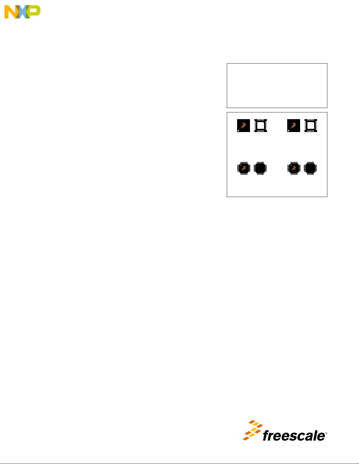
MKL15ZxxVFM4
MKL15ZxxVFT4
MKL15ZxxVLH4
MKL15ZxxVLK4
32-pin QFN (FM)
5 x 5 x 1 Pitch 0.5 mm
48-pin QFN (FT)
7 x 7 x 1 Pitch 0.5 mm
64-pin LQFP (LH)
10 x 10 x 1.4 Pitch 0.5
mm
80-pin LQFP (LK)
12 x 12 x 1.4 Pitch 0.5
mm
Freescale Semiconductor, Inc.
Document Number: KL15P80M48SF0
Data Sheet: Technical Data Rev 5 08/2014
Freescale reserves the right to change the detail specifications as may be required to
permit improvements in the design of its products. © 2012–2014 Freescale
Semiconductor, Inc. All rights reserved.
Ordering Information
Part Number Memory Maximum number of I\O's
Flash (KB) SRAM (KB)
MKL15Z32VFM4 32 4 28
MKL15Z64VFM4 64 8 28
MKL15Z128VFM4 128 16 28
MKL15Z32VFT4 32 4 40
MKL15Z64VFT4 64 8 40
MKL15Z128VFT4 128 16 40
MKL15Z32VLH4 32 4 54
MKL15Z64VLH4 64 8 54
MKL15Z128VLH4 128 16 54
MKL15Z32VLK4 32 4 70
MKL15Z64VLK4 64 8 70
MKL15Z128VLK4 128 16 70
Related Resources
Type Description Resource
Selector Guide The Freescale Solution Advisor is a web-based tool that features
interactive application wizards and a dynamic product selector.
Solution Advisor
Product Brief The Product Brief contains concise overview/summary information to
enable quick evaluation of a device for design suitability.
KL1 Family Product Brief
1
Reference
Manual
The Reference Manual contains a comprehensive description of the
structure and function (operation) of a device.
KL15P80M48SF0RM
1
Data Sheet The Data Sheet includes electrical characteristics and signal
connections.
KL15P80M48SF0
1
Chip Errata The chip mask set Errata provides additional or corrective
information for a particular device mask set.
KINETIS_L_xN97F
2
Package
drawing
Package dimensions are provided in package drawings. QFN 32-pin: 98ASA00473D
1
QFN 48-pin: 98ASA00466D
1
LQFP 64-pin: 98ASS23234W
1
LQFP 80-pin: 98ASS23174W
1
1. To find the associated resource, go to http://www.freescale.com and perform a search using this term.
2. To find the associated resource, go to http://www.freescale.com and perform a search using this term with the “x”
replaced by the revision of the device you are using.
Figure 1 shows the functional modules in the chip.
2
Kinetis KL15 Sub-Family, Rev5 08/2014.
Freescale Semiconductor, Inc.
Memories and
Memory Interfaces
Program
flash
RAM
6-bit DAC
Analog
Timers
Communication
Interfaces
Security
and Integrity
SPI
x2
Low
power timer
Clocks
Phase-
Core
Debug
interfaces
Interrupt
controller
comparator
x1
Analog
Human-Machine
Interface (HMI)
System
DMA
Internal
watchdog
locked loop
reference
Internal
clocks
timers
interrupt
Periodic
oscillator
Low/high
frequency
Low power
UART
x1
Cortex-M0+
ARM
with
GPIOs
interrupt
Kinetis KL15 Family
LEGEND
x2
I C
2
x1
Timers
1x6ch+2x2ch
16-bit ADC
x1
TSI
12-bit DAC
UART
x2
Migration difference from KL05 family
BME
MTB
RTC
watchdog
Internal
Frequency-
locked loop
Figure 1. Functional block diagram
Kinetis KL15 Sub-Family, Rev5 08/2014.
3
Freescale Semiconductor, Inc.
Table of Contents
1 Ratings....................................................................................5
1.1 Thermal handling ratings................................................. 5
1.2 Moisture handling ratings................................................ 5
1.3 ESD handling ratings.......................................................5
1.4 Voltage and current operating ratings............................. 5
2 General................................................................................... 6
2.1 AC electrical characteristics.............................................6
2.2 Nonswitching electrical specifications..............................6
2.2.1 Voltage and current operating requirements....... 7
2.2.2 LVD and POR operating requirements................7
2.2.3 Voltage and current operating behaviors.............8
2.2.4 Power mode transition operating behaviors........ 9
2.2.5 Power consumption operating behaviors............ 10
2.2.6 EMC radiated emissions operating behaviors.....15
2.2.7 Designing with radiated emissions in mind..........16
2.2.8 Capacitance attributes.........................................16
2.3 Switching specifications...................................................16
2.3.1 Device clock specifications..................................16
2.3.2 General switching specifications......................... 17
2.4 Thermal specifications.....................................................17
2.4.1 Thermal operating requirements......................... 17
2.4.2 Thermal attributes................................................18
3 Peripheral operating requirements and behaviors.................. 18
3.1 Core modules.................................................................. 18
3.1.1 SWD electricals .................................................. 18
3.2 System modules.............................................................. 20
3.3 Clock modules................................................................. 20
3.3.1 MCG specifications..............................................20
3.3.2 Oscillator electrical specifications........................22
3.4 Memories and memory interfaces................................... 24
3.4.1 Flash electrical specifications..............................24
3.5 Security and integrity modules........................................ 26
3.6 Analog............................................................................. 26
3.6.1 ADC electrical specifications............................... 26
3.6.2 CMP and 6-bit DAC electrical specifications....... 31
3.6.3 12-bit DAC electrical characteristics....................32
3.7 Timers..............................................................................35
3.8 Communication interfaces............................................... 35
3.8.1 SPI switching specifications................................ 35
3.8.2 Inter-Integrated Circuit Interface (I2C) timing...... 40
3.8.3 UART...................................................................41
3.9 Human-machine interfaces (HMI)....................................41
3.9.1 TSI electrical specifications................................. 41
4 Dimensions............................................................................. 42
4.1 Obtaining package dimensions....................................... 42
5 Pinout......................................................................................42
5.1 KL15 Signal Multiplexing and Pin Assignments...............42
5.2 KL15 pinouts....................................................................45
6 Ordering parts......................................................................... 49
6.1 Determining valid orderable parts....................................49
7 Part identification.....................................................................49
7.1 Description.......................................................................50
7.2 Format............................................................................. 50
7.3 Fields............................................................................... 50
7.4 Example...........................................................................50
8 Terminology and guidelines.................................................... 51
8.1 Definition: Operating requirement....................................51
8.2 Definition: Operating behavior......................................... 51
8.3 Definition: Attribute.......................................................... 52
8.4 Definition: Rating............................................................. 52
8.5 Result of exceeding a rating............................................ 52
8.6 Relationship between ratings and operating
requirements....................................................................53
8.7 Guidelines for ratings and operating requirements..........53
8.8 Definition: Typical value...................................................54
8.9 Typical value conditions.................................................. 55
9 Revision history.......................................................................55
4
Kinetis KL15 Sub-Family, Rev5 08/2014.
Freescale Semiconductor, Inc.
1 Ratings
1.1 Thermal handling ratings
Table 1. Thermal handling ratings
Symbol Description Min. Max. Unit Notes
T
STG
Storage temperature –55 150 °C 1
T
SDR
Solder temperature, lead-free — 260 °C 2
1. Determined according to JEDEC Standard JESD22-A103, High Temperature Storage Life.
2. Determined according to IPC/JEDEC Standard J-STD-020, Moisture/Reflow Sensitivity Classification for Nonhermetic
Solid State Surface Mount Devices.
1.2 Moisture handling ratings
Table 2. Moisture handling ratings
Symbol Description Min. Max. Unit Notes
MSL Moisture sensitivity level — 3 — 1
1. Determined according to IPC/JEDEC Standard J-STD-020, Moisture/Reflow Sensitivity Classification for Nonhermetic
Solid State Surface Mount Devices.
1.3 ESD handling ratings
Table 3. ESD handling ratings
Symbol Description Min. Max. Unit Notes
V
HBM
Electrostatic discharge voltage, human body model –2000 +2000 V 1
V
CDM
Electrostatic discharge voltage, charged-device
model
–500 +500 V 2
I
LAT
Latch-up current at ambient temperature of 105 °C –100 +100 mA 3
1. Determined according to JEDEC Standard JESD22-A114, Electrostatic Discharge (ESD) Sensitivity Testing Human
Body Model (HBM).
2. Determined according to JEDEC Standard JESD22-C101, Field-Induced Charged-Device Model Test Method for
Electrostatic-Discharge-Withstand Thresholds of Microelectronic Components.
3. Determined according to JEDEC Standard JESD78, IC Latch-Up Test.
Ratings
Kinetis KL15 Sub-Family, Rev5 08/2014.
5
Freescale Semiconductor, Inc.
剩余56页未读,继续阅读
华亚军
- 粉丝: 0
- 资源: 3
上传资源 快速赚钱
- 我的内容管理 展开
- 我的资源 快来上传第一个资源
- 我的收益 登录查看自己的收益
- 我的积分 登录查看自己的积分
- 我的C币 登录后查看C币余额
- 我的收藏
- 我的下载
- 下载帮助
安全验证
文档复制为VIP权益,开通VIP直接复制
信息提交成功
评论0