

Non-Isolated DC/DC Boost Converter
University of Alberta
ECE 730 Project Report 1
By: Faraz Ahmad – 1238006
To: Dr. Yunwei (Ryan) Li
Submitted on: Oct 13, 2009

2
Abstract
This report presents the working principle and performance of non-isolated
DC/DC Boost Converter with a method of boosting DC voltage from 12 Volts to
60 Volts. To perform the operation of the circuit, the simulation software
Matlab/Simulink is utilized. The output voltage and current wave forms are
observed under study state condition for different load conditions. Up to 50%
load change, the inductor operates in the continuous conduction mode however
when the load is increased to 10% of its initial value the inductor current goes
below zero thereby operating in discontinuous conduction mode .In DCM
operation the output voltage is almost doubled .To ensure the constant output
voltage the control signal is changed according to the discontinuous conduction
of the circuit.

3
1. Introduction
1.1 Study Initiatives
Efficiency, size, and cost are the primary advantages of switching power
converters when compared to linear converters. Switching power converter
efficiencies can run between 70-80%, whereas linear converters are usually 30%
efficient. The DC-DC Switching Boost Converter is designed to provide an
efficient method of taking a given DC voltage supply and boosting it to a desired
value.
1.2 Problem Definition
This project focuses on the study of non-isolated DC to DC boost
converter. The input voltage is 12 volts with a constant output voltage of 60 volts.
The frequency of operation is 20 kHz (i.e. switching frequency) while the output
power is 240 watt and the boundary condition between continuous and
discontinuous conduction modes occurs at 40 % of full load. The circuit is to be
analyzed for three different cases (1) Full load in steady state (2) Transient of
load step change from 100% to 50% of full load and (3) Transient of load step
change from 100% to 10% of full load
1.3 Approach of study
The inductor current waveform is to be studied under steady state
condition so using voltage second balancing principle; equations are to be
derived for the output current and voltage in terms of the control signal and the
passive circuit parameters. After the calculations of circuit elements, the circuit is
modeled in Simulink.
2. Theory
2.1 Basic operation
The boost converter outputs the voltage that is greater then the input voltage.
The schematic diagram is shown in the figure.1. It consists of the DC input
voltage, boost inductor, diode, the control switch (IGBT Switch), filter capacitor
and load resistor.
When the switch is closed, the diode is reversed biased and the current is being
drawn through the inductor linearly. At this time energy is being stored in the
inductor. When the switch is OFF, the energy stored in the inductor is released
through the diode to the RC circuit. So the output stage receives energy from the
inductor as well as the input stage.

4
Figure 1: DC/DC boost converter
2.2 Circuit Analysis
2.2.1 Continuous conduction mode
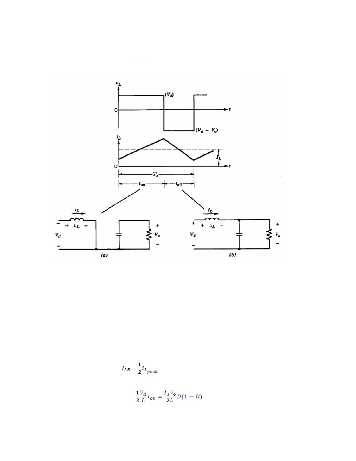
The converter waveforms in the Continuous Conduction Mode i.e. when
the inductor current is greater then zero is shown in figure 2.Applying the voltage
second balancing principle to the inductor voltage waveform.
0)( ��� toffVoVdVd
Dividing both sides by the switching time period and rearranging
……………….Eq.1
Where Ts = t (on) +t (off) and D is the Duty ratio defined as the ratio of the ON
duration to the switching time period Ts.
s
on
T
t
D �
Considering the ideal condition, i.e. there are no loses,
Pd = Po
oodd
IVIV �
5
)1(
0
D
I
I
d
��
……………… Eq.2
Figure 2: Continuous Conduction Mode :(a) Switch On; (b) Switch off
2.2.2 Boundary between Continuous & Discontinuous conduction modes:
Boundary condition exists when the inductor current goes to zero. As
shown in figure 3, at the boundary, the average value of the inductor current is
LB
I
= …………..Eq.3