


a
Blackfin and the Blackfin logo are registered trademarks of Analog Devices, Inc.
Blackfin
®
Embedded Processor
ADSP-BF533
Rev. D
Information furnished by Analog Devices is believed to be accurate and reliable.
However, no responsibility is assumed by Analog Devices for its use, nor for any
infringements of patents or other rights of third parties that may result from its use.
Specifications subject to change without notice. No license is granted by implication
or otherwise under any patent or patent rights of Analog Devices. Trademarks and
registered trademarks are the property of their respective owners.
One Technology Way, P.O. Box 9106, Norwood, MA 02062-9106 U.S.A.
Tel: 781.329.4700 www.analog.com
Fax: 781.461.3113 © 2006 Analog Devices, Inc. All rights reserved.
FEATURES
Up to 600 MHz high performance Blackfin processor
Two 16-bit MACs, two 40-bit ALUs, four 8-bit video ALUs,
40-bit shifter
RISC-like register and instruction model for ease of pro-
gramming and compiler-friendly support
Advanced debug, trace, and performance monitoring
0.8 V to 1.26 V core V
DD
with on-chip voltage regulation
1.8 V, 2.5 V, and 3.3 V compliant I/O
160-ball mini-BGA, 169-ball lead free PBGA packages
MEMORY
Up to 148K bytes of on-chip memory:
16K bytes of instruction SRAM/Cache
64K bytes of instruction SRAM
32K bytes of data SRAM/Cache
32K bytes of data SRAM
4K bytes of scratchpad SRAM
Two dual-channel memory DMA controllers
Memory management unit providing memory protection
External memory controller with glueless support for
SDRAM, SRAM, FLASH, and ROM
Flexible memory booting options from SPI
®
and
external memory
PERIPHERALS
Parallel peripheral interface PPI/GPIO, supporting
ITU-R 656 video data formats
Two dual-channel, full duplex synchronous serial ports, sup-
porting eight stereo I
2
S channels
12-channel DMA controller
SPI-compatible port
Three timer/counters with PWM support
UART with support for IrDA
®
Event handler
Real-time clock
Watchdog timer
Debug/JTAG interface
On-chip PLL capable of 0.5ⴛ to 64ⴛ frequency multiplication
Core timer
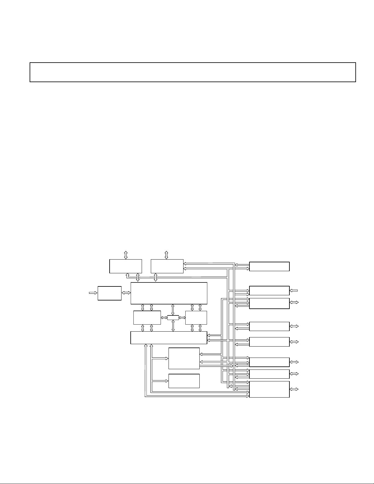
Figure 1. Functional Block Diagram
VOLTAGE
REGULATOR
DMA
CONTROLLER
EVENT
CONTROLLER/
CORE TIMER
REAL-TIME CLOCK
UART PORT
IrDA
TIMER0, TIMER1,
TIMER2
PPI / GPIO
SERIAL PORTS (2)
SPI PORT
EXTERNAL PORT
FLASH, SDRAM
CONTROL
BOOT ROM
JTAG TEST AND
EMULATION
WATCHDOG TIMER
L1
INSTRUCTION
MEMORY
L1
DATA
MEMORY
MMU
CORE/SYSTEM BUS INTERFACE
B

Rev. D | Page 2 of 60 | September 2006
ADSP-BF533
TABLE OF CONTENTS
General Description ................................................. 4
Portable Low Power Architecture ............................. 4
System Integration ................................................ 4
ADSP-BF533 Processor Peripherals ........................... 4
Blackfin Processor Core .......................................... 4
Memory Architecture ............................................ 5
DMA Controllers .................................................. 8
Real-Time Clock ................................................... 9
Watchdog Timer .................................................. 9
Timers ............................................................... 9
Serial Ports (SPORTs) .......................................... 10
Serial Peripheral Interface (SPI) Port ....................... 10
UART Port ........................................................ 10
Programmable Flags (PFx) .................................... 11
Parallel Peripheral Interface ................................... 11
Dynamic Power Management ................................ 11
Voltage Regulation .............................................. 13
Clock Signals ..................................................... 13
Booting Modes ................................................... 14
Instruction Set Description ................................... 14
Development Tools ............................................. 15
Designing an Emulator-Compatible Processor Board .. 16
Related Documents ............................................. 16
Pin Descriptions .................................................... 17
Specifications ........................................................ 20
Operating Conditions .......................................... 20
Electrical Characteristics ....................................... 21
Absolute Maximum Ratings .................................. 22
Package Information ........................................... 22
ESD Sensitivity ................................................... 22
Timing Specifications .......................................... 23
Clock and Reset Timing .................................... 24
Asynchronous Memory Read Cycle Timing ........... 25
Asynchronous Memory Write Cycle Timing .......... 26
SDRAM Interface Timing .................................. 27
External Port Bus Request and Grant Cycle Timing .. 28
Parallel Peripheral Interface Timing ..................... 29
Serial Ports ..................................................... 32
Serial Peripheral Interface (SPI) Port
—Master Timing .......................................... 37
Serial Peripheral Interface (SPI) Port
—Slave Timing ............................................. 38
Universal Asynchronous Receiver-Transmitter
(UART) Port—Receive and Transmit Timing ...... 39
Programmable Flags Cycle Timing ....................... 40
Timer Cycle Timing .......................................... 41
JTAG Test and Emulation Port Timing .................. 42
Output Drive Currents ......................................... 43
Power Dissipation ............................................... 45
Test Conditions .................................................. 45
Environmental Conditions .................................... 48
160-Ball BGA Pinout ............................................... 50
169-Ball PBGA Pinout ............................................. 53
Outline Dimensions ................................................ 56
Ordering Guide ..................................................... 58

ADSP-BF533
Rev. D | Page 3 of 60 | September 2006
REVISION HISTORY
8/06—Revision D: Changed from Rev. C to Rev. D
Added 1.8 V I/O to Features ....................................... 1
Changed Text in Figure External Components for RTC .... 9
Added Text to Serial Ports (SPORTs) ........................... 10
Changed Font in Formula in Power Savings .................. 12
Complete Rewrite of Operating Conditions ................... 20
Added 1.8 V to Operating Conditions .......................... 20
Complete Rewrite of Electrical Characteristics ............... 21
Added 1.8 V Specifications to Multiple Tables of
Timing Specifications .............................................. 23
Edit to Asynchronous Memory Read Cycle Timing ......... 25
Edit to Asynchronous Memory Write Cycle Timing ........ 26
Changed Data in SDRAM Interface Timing .................. 27
Changed Data in Parallel Peripheral Interface Timing ...... 29
Changed Data in Serial Ports ..................................... 32
Deleted References to Temperature in Figures
in Output Drive Currents ......................................... 43
Added 1.8 V Data to Output Drive Currents .................. 43
Moved Data to Operating Conditions
and Rewrote Power Dissipation ................................. 45
Deleted References to Temperature in Figures
in Test Conditions .................................................. 45
Added 1.8 V References in Test Conditions ................... 45
Added 1.8 V Characterization Data Capacitive Loading ... 45
Changed Thermal Characteristics for BC-160 Package ..... 49
Added Models to Ordering Guide ............................... 58

Rev. D | Page 4 of 60 | September 2006
ADSP-BF533
GENERAL DESCRIPTION
The ADSP-BF533 processor is a member of the Blackfin family
of products, incorporating the Analog Devices, Inc./Intel Micro
Signal Architecture (MSA). Blackfin processors combine a dual-
MAC state-of-the-art signal processing engine, the advantages
of a clean, orthogonal RISC-like microprocessor instruction set,
and single instruction, multiple data (SIMD) multimedia capa-
bilities into a single instruction set architecture.
The Blackfin processors are completely code and pin-compati-
ble, differing only with respect to their performance and on-
chip memory. Specific performance and memory configura-
tions are shown in Table 1.
By integrating a rich set of industry-leading system peripherals
and memory, Blackfin processors are the platform of choice for
next generation applications that require RISC-like program-
mability, multimedia support, and leading-edge signal
processing in one integrated package.
PORTABLE LOW POWER ARCHITECTURE
Blackfin processors provide world-class power management
and performance. Blackfin processors are designed in a low
power and low voltage design methodology and feature
dynamic power management—the ability to vary both the volt-
age and frequency of operation to significantly lower overall
power consumption. Varying the voltage and frequency can
result in a substantial reduction in power consumption, com-
pared with just varying the frequency of operation. This
translates into longer battery life for portable appliances.
SYSTEM INTEGRATION
The ADSP-BF533 processor is a highly integrated system-on-a-
chip solution for the next generation of digital communication
and consumer multimedia applications. By combining indus-
try-standard interfaces with a high performance signal
processing core, users can develop cost-effective solutions
quickly without the need for costly external components. The
system peripherals include a UART port, an SPI port, two serial
ports (SPORTs), four general-purpose timers (three with PWM
capability), a real-time clock, a watchdog timer, and a parallel
peripheral interface.
ADSP-BF533 PROCESSOR PERIPHERALS
The ADSP-BF533 processor contains a rich set of peripherals
connected to the core via several high bandwidth buses, provid-
ing flexibility in system configuration as well as excellent overall
system performance (see the functional block diagram in
Figure 1 on Page 1). The general-purpose peripherals include
functions such as UART, timers with PWM (pulse-width mod-
ulation) and pulse measurement capability, general-purpose
flag I/O pins, a real-time clock, and a watchdog timer. This set
of functions satisfies a wide variety of typical system support
needs and is augmented by the system expansion capabilities of
the part. In addition to these general-purpose peripherals, the
ADSP-BF533 processor contains high speed serial and parallel
ports for interfacing to a variety of audio, video, and modem
codec functions; an interrupt controller for flexible manage-
ment of interrupts from the on-chip peripherals or external
sources; and power management control functions to tailor the
performance and power characteristics of the processor and sys-
tem to many application scenarios.
All of the peripherals, except for general-purpose I/O, real-time
clock, and timers, are supported by a flexible DMA structure.
There is also a separate memory DMA channel dedicated to
data transfers between the processor’s various memory spaces,
including external SDRAM and asynchronous memory. Multi-
ple on-chip buses running at up to 133 MHz provide enough
bandwidth to keep the processor core running along with activ-
ity on all of the on-chip and external peripherals.
The ADSP-BF533 processor includes an on-chip voltage regula-
tor in support of the processor’s dynamic power management
capability. The voltage regulator provides a range of core volt-
age levels from a single 2.25 V to 3.6 V input. The voltage
regulator can be bypassed at the user’s discretion.
BLACKFIN PROCESSOR CORE
As shown in Figure 2 on Page 6, the Blackfin processor core
contains two 16-bit multipliers, two 40-bit accumulators, two
40-bit ALUs, four video ALUs, and a 40-bit shifter. The compu-
tation units process 8-bit, 16-bit, or 32-bit data from the
register file.
The compute register file contains eight 32-bit registers. When
performing compute operations on 16-bit operand data, the
register file operates as 16 independent 16-bit registers. All
operands for compute operations come from the multiported
register file and instruction constant fields.
Each MAC can perform a 16-bit by 16-bit multiply in each
cycle, accumulating the results into the 40-bit accumulators.
Signed and unsigned formats, rounding, and saturation are
supported.
The ALUs perform a traditional set of arithmetic and logical
operations on 16-bit or 32-bit data. In addition, many special
instructions are included to accelerate various signal processing
tasks. These include bit operations such as field extract and pop-
ulation count, modulo 2
32
multiply, divide primitives, saturation
and rounding, and sign/exponent detection. The set of video
Table 1. Processor Comparison
ADSP-BF533
Maximum Performance 600 MHz 1200 MMACs
Instruction
SRAM/Cache
16K bytes
Instruction SRAM 64K bytes
Data
SRAM/Cache
32K bytes
Data SRAM 32K bytes
Scratchpad 4K bytes

ADSP-BF533
Rev. D | Page 5 of 60 | September 2006
instructions includes byte alignment and packing operations,
16-bit and 8-bit adds with clipping, 8-bit average operations,
and 8-bit subtract/absolute value/accumulate (SAA) operations.
Also provided are the compare/select and vector search
instructions.
For certain instructions, two 16-bit ALU operations can be per-
formed simultaneously on register pairs (a 16-bit high half and
16-bit low half of a compute register). By also using the second
ALU, quad 16-bit operations are possible.
The 40-bit shifter can perform shifts and rotates and is used to
support normalization, field extract, and field deposit
instructions.
The program sequencer controls the flow of instruction execu-
tion, including instruction alignment and decoding. For
program flow control, the sequencer supports PC relative and
indirect conditional jumps (with static branch prediction), and
subroutine calls. Hardware is provided to support zero-over-
head looping. The architecture is fully interlocked, meaning that
the programmer need not manage the pipeline when executing
instructions with data dependencies.
The address arithmetic unit provides two addresses for simulta-
neous dual fetches from memory. It contains a multiported
register file consisting of four sets of 32-bit index, modify,
length, and base registers (for circular buffering), and eight
additional 32-bit pointer registers (for C-style indexed stack
manipulation).
Blackfin processors support a modified Harvard architecture in
combination with a hierarchical memory structure. Level 1 (L1)
memories are those that typically operate at the full processor
speed with little or no latency. At the L1 level, the instruction
memory holds instructions only. The two data memories hold
data, and a dedicated scratchpad data memory stores stack and
local variable information.
In addition, multiple L1 memory blocks are provided, offering a
configurable mix of SRAM and cache. The memory manage-
ment unit (MMU) provides memory protection for individual
tasks that may be operating on the core and can protect system
registers from unintended access.
The architecture provides three modes of operation: user mode,
supervisor mode, and emulation mode. User mode has
restricted access to certain system resources, thus providing a
protected software environment, while supervisor mode has
unrestricted access to the system and core resources.
The Blackfin processor instruction set has been optimized so
that 16-bit opcodes represent the most frequently used instruc-
tions, resulting in excellent compiled code density. Complex
DSP instructions are encoded into 32-bit opcodes, representing
fully featured multifunction instructions. Blackfin processors
support a limited multi-issue capability, where a 32-bit instruc-
tion can be issued in parallel with two 16-bit instructions,
allowing the programmer to use many of the core resources in a
single instruction cycle.
The Blackfin processor assembly language uses an algebraic syn-
tax for ease of coding and readability. The architecture has been
optimized for use in conjunction with the C/C++ compiler,
resulting in fast and efficient software implementations.
MEMORY ARCHITECTURE
The Blackfin processors view memory as a single unified
4G byte address space, using 32-bit addresses. All resources,
including internal memory, external memory, and I/O control
registers, occupy separate sections of this common address
space. The memory portions of this address space are arranged
in a hierarchical structure to provide a good cost/performance
balance of some very fast, low latency on-chip memory as cache
or SRAM, and larger, lower cost and performance off-chip
memory systems. See Figure 3 on Page 7.
The L1 memory system is the primary highest performance
memory available to the Blackfin processor. The off-chip mem-
ory system, accessed through the external bus interface unit
(EBIU), provides expansion with SDRAM, flash memory, and
SRAM, optionally accessing up to 132M bytes of
physical memory.
The memory DMA controller provides high bandwidth data-
movement capability. It can perform block transfers of code or
data between the internal memory and the external
memory spaces.
Internal (On-Chip) Memory
The ADSP-BF533 processor has three blocks of on-chip mem-
ory providing high bandwidth access to the core.
The first is the L1 instruction memory, consisting of up to
80K bytes SRAM, of which 16K bytes can be configured as a
four way set-associative cache. This memory is accessed at full
processor speed.
The second on-chip memory block is the L1 data memory, con-
sisting of up to two banks of up to 32K bytes each. Each memory
bank is configurable, offering both cache and SRAM functional-
ity. This memory block is accessed at full processor speed.
The third memory block is a 4K byte scratchpad SRAM which
runs at the same speed as the L1 memories, but is only accessible
as data SRAM and cannot be configured as cache memory.
External (Off-Chip) Memory
The external bus interface can be used with both asynchronous
devices such as SRAM, FLASH, EEPROM, ROM, and I/O
devices, and synchronous devices such as SDRAMs. The bus
width is always 16 bits. A1 is the least significant address of a
16-bit word. 8-bit peripherals should be addressed as if they
were 16-bit devices, where only the lower eight bits of data
should be used.
The PC133-compliant SDRAM controller can be programmed
to interface to up to 128M bytes of SDRAM. The SDRAM con-
troller allows one row to be open for each internal SDRAM
bank, for up to four internal SDRAM banks, improving overall
system performance.


