没有合适的资源?快使用搜索试试~ 我知道了~
资源详情
资源评论
资源推荐
Engineer-to-Engineer Note EE-240
a
Technical notes on using Analog Devices DSPs, Processors and development tools
Contact our technical support at dsp.support@analog.com and at dsptools.support@analog.com
Or visit our on-line resources http://www.analog.com/ee-notes and http://www.analog.com/Processors
ADSP-BF533 Blackfin® Booting Process
Contributed by Hiren Desai Rev 1 – June 3, 2004
Copyright 2004, Analog Devices, Inc. All rights reserved. Analog Devices assumes no responsibility for customer product design or the use or application of
customers’ products or for any infringements of patents or rights of others which may result from Analog Devices assistance. All trademarks and logos are property
Introduction
This EE-Note describes the booting process for the ADSP-BF531, ADSP-BF532, and ADSP-BF533
Blackfin
®
processors. Differences between silicon revision levels are noted.
This EE-Note discusses:
! Boot modes
! Loader file header information
! Initialization code
! Multi-application (multi-DXE) management
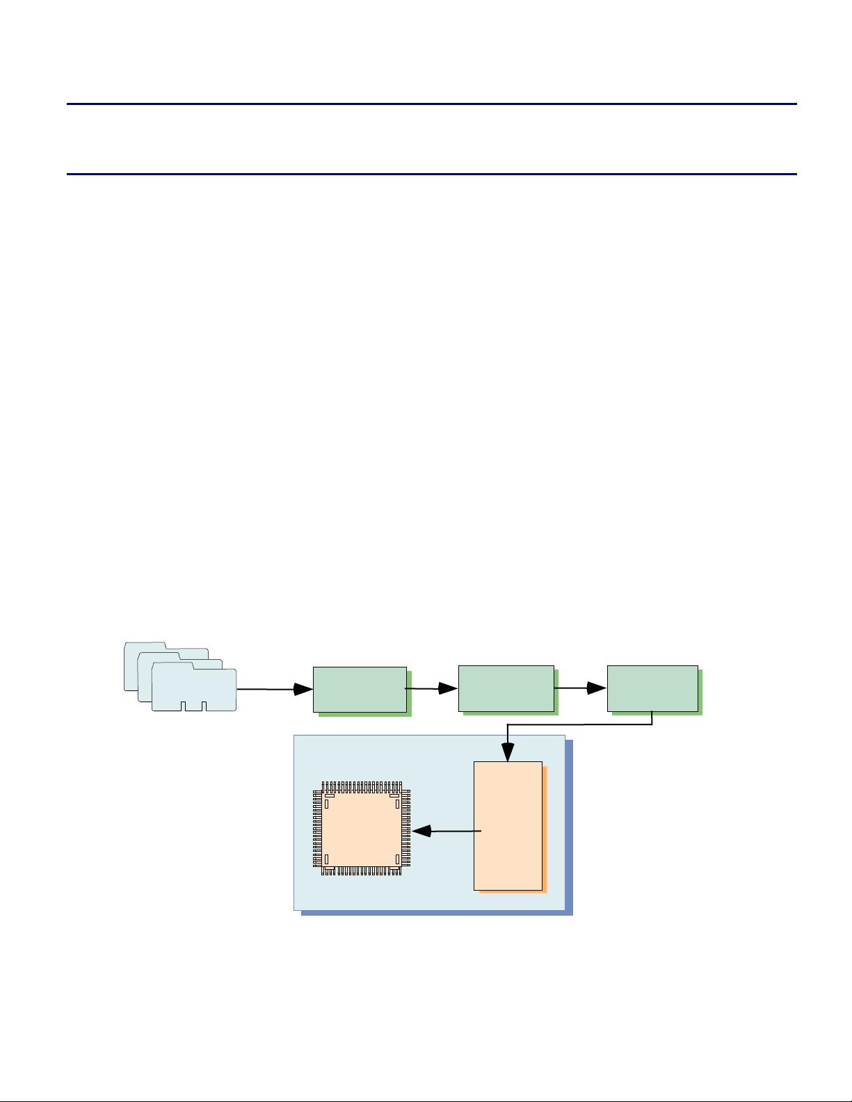
The Booting Process
Booting is the process of loading application code/data, stored in an external memory device (or external
host), into the various internal and external memories of the Blackfin processor. This is handled by the on-
chip boot ROM which is located in Blackfin memory at address
0xEF00 0000 to 0xEF00 03FF. Figure 1
shows the sequence of operations taken from source code to the final target stand-alone system.
Figure 1. ADSP-BF531/BF532/BF533 Stand-Alone System
ADSP-BF53x
Processor
Booting
Upon
RESET
Target System
External
Memory
Assembler and/or
Compiler
Linker
Loader
Source Files
.ASM, .C, .CPP
.DXE(s)
.DOJ(s)
.LDR
of their respective holders. Information furnished by Analog Devices applications and development tools engineers is believed to be accurate and reliable, however
no responsibility is assumed by Analog Devices regarding technical accuracy and topicality of the content provided in Analog Devices’ Engineer-to-Engineer Notes.
a
Boot Modes (Silicon Revision 0.3)*
Blackfin processors can boot from a flash/PROM via asynchronous Bank 0 of the EBIU or an SPI device
(memory or host) via the SPI interface. Table 1 lists ADSP-BF531/BF532/BF533 processor booting
modes, which are selected by the state of the BMODE[1:0] pins when the
RESET signal is de-asserted.
BMODE[1:0] Description (See Also Specific Blackfin Boot Modes on page 10
00 Executes from external 16-bit memory connected to ASYNC Bank0 (bypass boot ROM)
01 Boots from 8/16-bit flash/PROM
10 Boots from a SPI host in SPI Slave mode
11 Boots from a 8/16/24-bit addressable SPI memory in SPI Master mode with support for
Atmel AT45DB041B, AT45DB081B, and AT45DB161B DataFlash® devices
Table 1. Blackfin ADSP-BF531/BF532/BF533 Booting Modes
* For boot modes supported on previous revisions of silicon, refer to the
Appendix: Boot Modes vs. Silicon Revisions.
As Figure 1 illustrates, the loader utility (elfloader.exe) parses the input executable file (.DXE) and
creates a loader file (
.LDR)*, consisting of blocks preceded by headers. This loader file is then
programmed/burned into the external memory/device. The headers are read and parsed by the on-chip
boot ROM during booting.
* Refer to the VisualDSP++ 3.5 Loader Manual for 16-Bit Processors [1] for information on switches loader files
Loader File is programmed/burned into the External Memory/Device
ADSP-BF531/BF532/BF533 Processor
Figure 2. ADSP-BF531/BF532/BF533 Boot Process
!
Booting into scratchpad memory (0xFFB0 0000 – 0xFFB0 0FFF) is not supported. If booting to
scratchpad memory is attempted, the processor will hang within the on-chip boot ROM.
10-B
y
te Header for Block 2
10-B
y
te Header for Block 3
Block 2
Block 3
10-B
y
te Header for Block n
Block n
……………..
Loader File
10-B
y
te Header for Block 1
Block 1
Block 1
L1 Memory
0xEF00 0000
...........
Flash/PROM or SPI
10-Byte Header for Block 1
Block 1
Block 2
10-Byte Header for Block 2
Block 3
App.
Code/
Data
Block 3
10-Byte Header for Block 3
10-Byte Header for ock n Bl
Block n
On-Chip Boot
ROM
SDRAM
Block 2
ADSP-BF533 Blackfin® Booting Process (EE-240) Page 2 of 28
a
Header Information
As shown in Figure 3, each 10-byte header within the loader file consists of a 4-byte ADDRESS field, a 4-
byte COUNT field, and a 2-byte FLAG field.
10-B
y
te Header for Block 1
Figure 3. 10-Byte Header Contents
This 10-byte header, which precedes each block in the loader file, contains the following information used
by the on-chip boot ROM during the boot process:
! ADDRESS (4 bytes) – the target address, to which the block will be booted within memory
! COUNT (4 bytes) – the number of bytes in the block
! FLAG (2 bytes) – block type and control commands:
FINAL
0 - Non-Last Block
1 - Last Block
PFLAG 3:0
PF number for
SPI slave booting
IGNORE
0 - Non-Ignore Block
1 - Ignore Block
INIT
0 - Non-Init Block
1 - Init Block
ZEROFILL
0 - Non-Zero Fill Block
1 - Zero-Fill Block
RESVECT
0 - ADSP-BF531/BF532
1 - ADSP-BF533
15 14 13 12 11 10 9 8 7 6 5 4 3 2 1 0
Figure 4. Individual Control Bits of the FLAG Word
10-B
y
te Header for Block 2
10-B
y
te Header for Block 3
10-B
y
te Header for Block n
Block 1
Block 2
Block 3
……………..
16-Bit FLAG
32-Bit ADDRESS
32-Bit COUNT
ADSP-BF533 Blackfin® Booting Process (EE-240) Page 3 of 28
a
The FLAG bits include:
" Bit 0: ZEROFILL - Indicates that the block is a buffer with zeros. ZEROFILL blocks have no
payload data. They simply instruct the on-chip boot ROM to zero COUNT bytes starting from
ADDRESS in memory. This yields a condensed loader file for applications with large zero buffers.
It is also very helpful for ANSI-C compliant projects which often require large buffers to be
zeroed during boot time.
" Bit 1: RESVECT – Indicates the reset vector after booting. All ADSP-BF531/BF532/BF533
derivatives use the same boot ROM. This bit is set to 0 for the ADSP-BF531/BF532 and it is set to
1 for the ADSP-BF533. After booting is complete, the on-chip boot ROM uses this bit to jump to
address
0xFFA0 0000 for the ADSP-BF533 or to address 0xFFA0 8000 for the ADSP-
BF531/BF532.
!
After a hardware reset, the reset vector (stored in the EVT1 register) is set to 0xFFA0 0000
or 0xFFA0 8000, depending on the RESVECT bit. If bit 4 (No Boot on Software Reset) of
the SYSCR register is set and a software reset is issued, the processor will vector to the
address set in the
EVT1 register. This reset vector can be reconfigured to another address
during runtime and hence, an application can vector to an address other than 0
xFFA0 0000
or
0xFFA0 8000 after a software reset. If the reset vector is modified during runtime,
ensure that the reset vector address within the EVT1 register is a valid instruction address.
This address can be internal instruction memory, SDRAM memory, or asynchronous
memory. The
EVT1 register does not have a default value. The value within this register
will be retained after a reset is issued. When BMODE = 00, the on-chip boot ROM is
bypassed and you must initialize the
EVT1 register before issuing a software reset.
" Bit 3: INIT – An initialization block (Init Block) is a block of code that executes before the actual
application code boots over it. When the on-chip boot ROM detects an Init Block, it boots the
block into internal memory and makes a CALL to it (initialization code must have an
RTS at the
end). After the initialization code is executed, it is typically overwritten with application code. See
Figure 5.
" Bit 4: IGNORE – Indicates a block that is not booted into memory. It instructs the boot ROM to
skip COUNT bytes of the boot stream. In master boot modes, the boot ROM can just modify its
source address pointer. In slave boot modes, the boot ROM must actively trash the payload data.
The current VisualDSP++® tools support IGNORE blocks for global headers only (currently the
4-byte DXE Count, see Multi-Application (Multi-DXE) Management section below).
" Bits 8:5: PFLAG - These bits are used for SPI Slave mode boot (BMODE = 10). PFLAG
indicates the
PF number used for the feedback strobe from the Blackfin processor to the Master
SPI host. This value can be between 1 – 15 (
0x1 – 0xF) for ADSP-BF531/BF532/BF533
processors. Refer to the SPI Slave Mode Boot via Master Host (BMODE = 10) section below for
further information on the usage of this PF strobe.
" Bit 15: FINAL – Indicates boot process is complete after this block. After processing a FINAL
block, the on-chip boot ROM jumps to the reset vector address stored in the
EVT1 register. The
processor is still in Supervisor mode and in the lowest priority interrupt (
IVG15) when it jumps to
L1 memory for code execution.
ADSP-BF533 Blackfin® Booting Process (EE-240) Page 4 of 28
a
!
Unlike ADSP-BF535 processors, ADSP-BF531/BF532/BF533 processors do not require a second-
stage loader. The FLAG field of the 10-byte header provides ADSP-BF531/BF532/BF533
processors with all the information needed to execute a single-stage boot sequence without the
need for a second-stage loader.
Initialization Code (Init Code)
Init Code is a feature that allows the execution of a piece code before the actual application is booted in.
This code can serve a number of purposes including initializing the SDRAM controller, or changing PLL
settings, the SPI baud rate, or EBIU wait states for faster boot time, etc. The Init Code is added to the
beginning of the loader file stream via the elfloader
–Init Init_Code.DXE command-line switch, where
Init_Code.DXE refers to the user-provided custom initialization code executable.
ADSP-BF531/BF532/BF533 Processor
Flash/PROM or SPI Device
Figure 5. Initialization Code Execution / Boot
When the on-chip boot ROM detects a block with the INIT bit set, it will first boot it into Blackfin
memory and then execute it, by issuing a CALL to its target address. For this reason, you must terminate
Header for Init Block
App.
Code/
Data
Init Block
A
L1 Memory
Init Block
Header for L1 Block
L1 Block
Header for SDRAM Block
SDRAM Block
........
0xEF00 0000
SDRAM
Header for Block n
Block n
On-Chip Boot
ROM
ADSP-BF531/BF532/BF533 Processor
Flash/PROM or SPI Device
After Init Code
Execution
A
Header for Init B cklo
Init Block
L1
Init Block
L1 Block
Header for L1 B cklo
L1 Block
App.
Code/
Data
Header for SDRAM B k
. . . . . . . .
loc
SDRAM Block
Header for Blo nck
Block n
0xEF00 0000
SDRAM
On-Chip Boot
ROM
SDRAM Block
ADSP-BF533 Blackfin® Booting Process (EE-240) Page 5 of 28
剩余27页未读,继续阅读
ablha
- 粉丝: 1
- 资源: 5
上传资源 快速赚钱
- 我的内容管理 展开
- 我的资源 快来上传第一个资源
- 我的收益 登录查看自己的收益
- 我的积分 登录查看自己的积分
- 我的C币 登录后查看C币余额
- 我的收藏
- 我的下载
- 下载帮助
最新资源
- 校园帮项目,毕业设计/课程设计/javaWeb/SSM
- C++ plotting library,matplotlib-cpp-master.zip
- 案例源码matplotlib-examples-master.zip
- 基于JavaScript 实现的KMP 算法
- 基于C++实现二叉树的创建,遍历,添加,查找与删除
- 基于C语言实现二叉树的基本操作
- 毕业设计基于STM32的测量温度与压力的数据处理设计C语言完整源码+论文.zip
- 基于MATLAB的PCA算法人脸识别项目源码+GUI界面+说明文档.zip
- 基于STM32的测量温度与压力的数据处理设计源码+论文(毕业设计).zip
- Vision Transformer 网络对不同氨气氧气浓度轨迹RAS 图像数据集的分类,包含训练权重和数据集、迁移学习
资源上传下载、课程学习等过程中有任何疑问或建议,欢迎提出宝贵意见哦~我们会及时处理!
点击此处反馈
安全验证
文档复制为VIP权益,开通VIP直接复制
信息提交成功
评论0