Altera Corporation 13–1
May 2007
13. Design Debugging Using
the SignalTap II Embedded
Logic Analyzer
Introduction
The phenomenal growth in design size and complexity continues to make
design verification a critical bottleneck for today's FPGA systems.
Limited access to internal signals, complex FPGA packages, and PCB
electrical noise all contribute to making design debugging the most
challenging process of the design cycle. More than 50% of the design cycle
time can be spent on debugging and verifying the design. To help with
the process of design debugging, Altera
®
provides a solution that enables
a designer to examine the behavior of internal signals, without using
extra I/O pins, while the design is running at full speed on an FPGA
device.
The SignalTap
®
II Embedded Logic Analyzer is scalable, easy to use, and
is included with the Quartus
®
II software subscription. This logic
analyzer helps debug an FPGA design by probing the state of the internal
signals in the design without the use of external equipment. Defining
custom trigger-condition logic provides greater accuracy and improves
the ability to isolate problems. The SignalTap II Embedded Logic
Analyzer does not require external probes, or changes to the design files
to capture the state of the internal nodes or I/O pins in the design. All
captured signal data is conveniently stored in device memory until the
designer is ready to read and analyze the data.
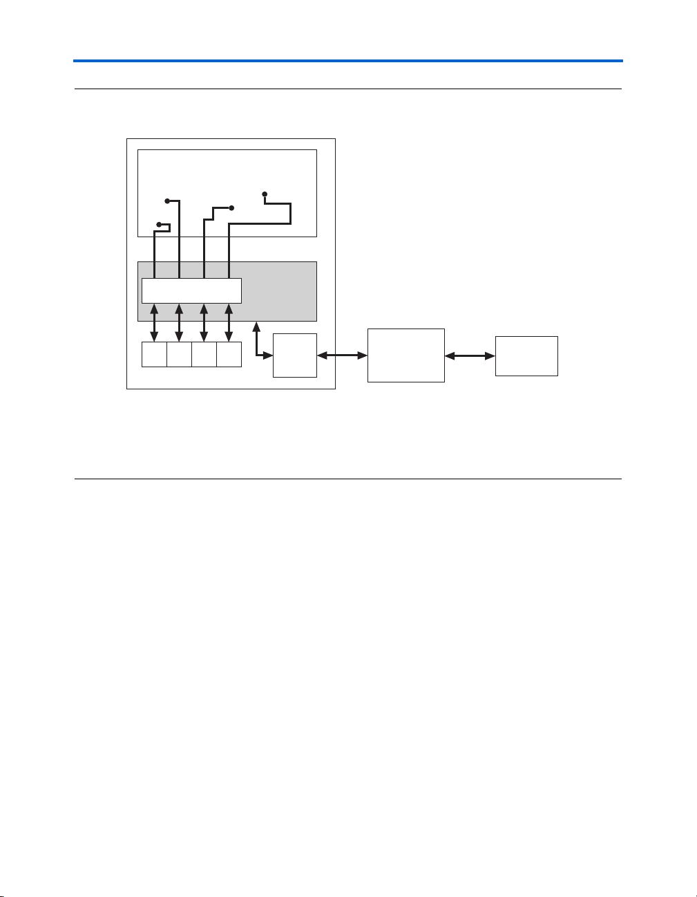
The SignalTap II Embedded Logic Analyzer is a next-generation
system-level debugging tool that captures and displays real-time signal
behavior in a system on a programmable chip (SOPC) or any FPGA
design. The SignalTap II Embedded Logic Analyzer supports the highest
number of channels, largest sample depth, and fastest clock speeds of any
embedded logic analyzer in the programmable logic market. Figure 13–1
shows a block diagram of the components that make up the SignalTap II
Embedded Logic Analyzer.
QII53009-7.1.0