


Low Power Nyquist-Rate ADCs
10 bit, 40 Ms/s, pipeline ADC design.
2.5 V, 0.25 µm CMOS.
J. Arias
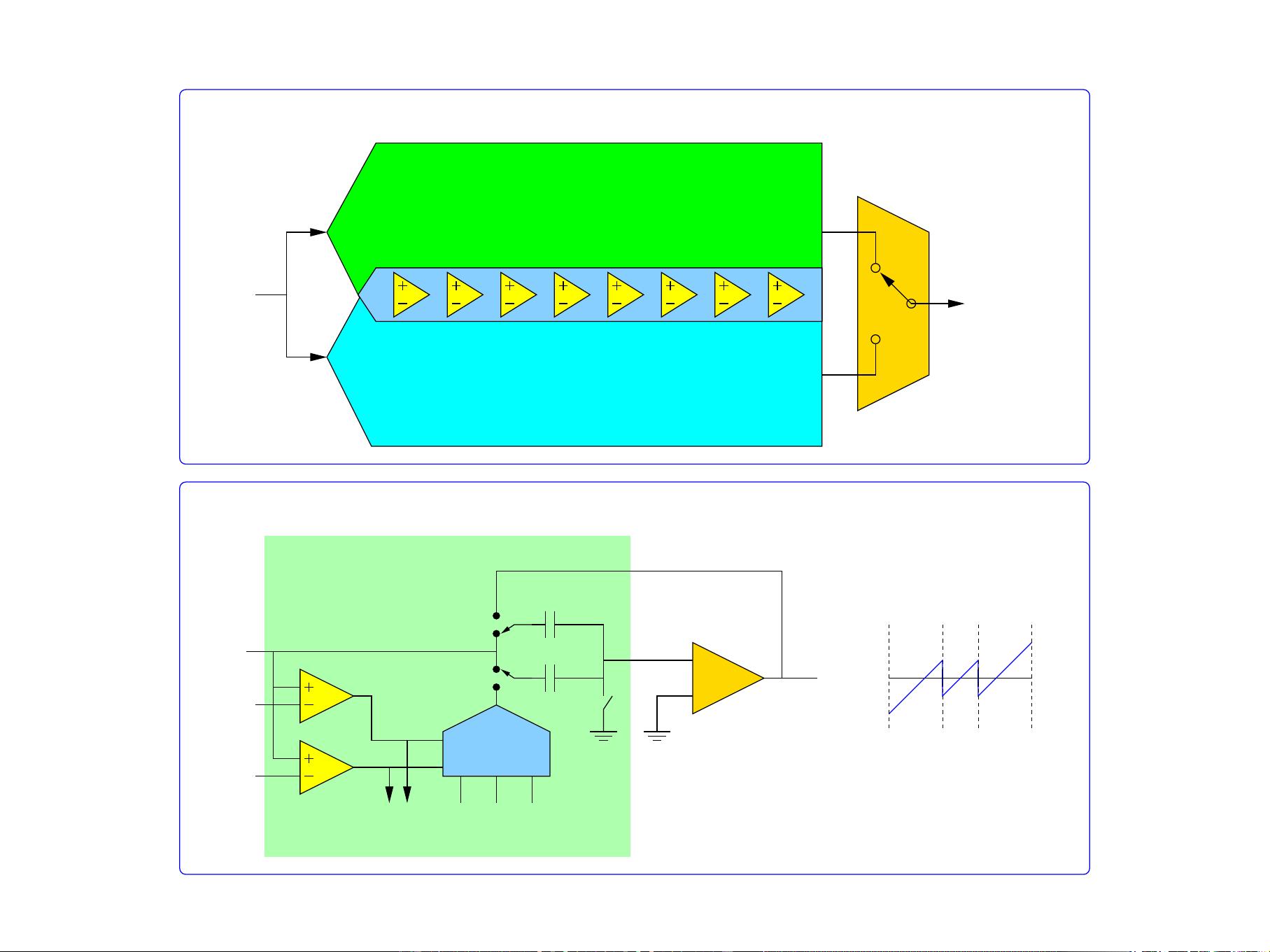
Global ADC achitecture:
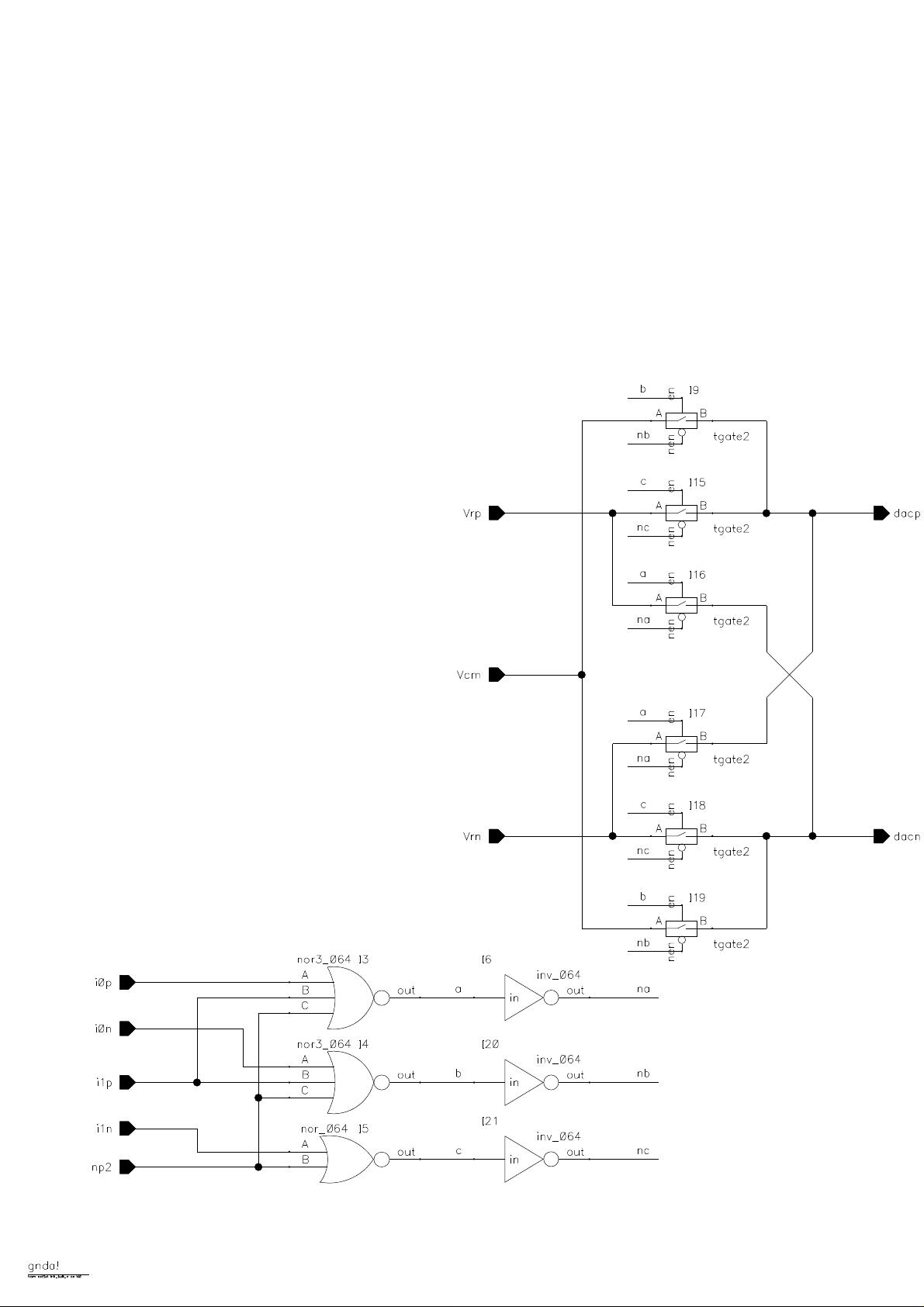
1.5 bits pipeline stage.
00 01 11
−Vref/4
+Vref/4
+
−
Cs
Cs
Input
Residue
Output
+Vref 0 −Vref
MUX
Digital
Output
+Vref+Vref/4
−Vref/4−Vref
Vo=2Vin−Vdac
1
2
1
1
2
Pipeline ADC
(even samples)
Pipeline ADC
(odd samples)
MUX
Vin
Dig. out.

Modifications to previous design
➯ Lower supply voltage: No enough room for a single cascode stage.
➯ New opamps are two-stages. This gives more DC gain and output swing, but stability
demands the use of compensation capacitors.
➯ Comparators need a new design to accommodate the new input range.
➯ Switches are fully CMOS transmission gates.

Opamps:
➯ Specs:
✔ Slew-rate high enough to charge the load capacitances in 1/4 of sampling period.
(SR 4V
swing
f
s
166V µs)
✔ Enough Unit-Gain Bandwidth to allow settling to 2
N
relative error in 1/4 of sampling
period. (GB
10f
s
200MHz)
✔ DC gain well over 2
N
to get good ADC linearity. (Gain>5000)
✔ Must be stable with a feedback factor about 1/2 (gain=2).
✔ Total opamp noise below quantization noise.
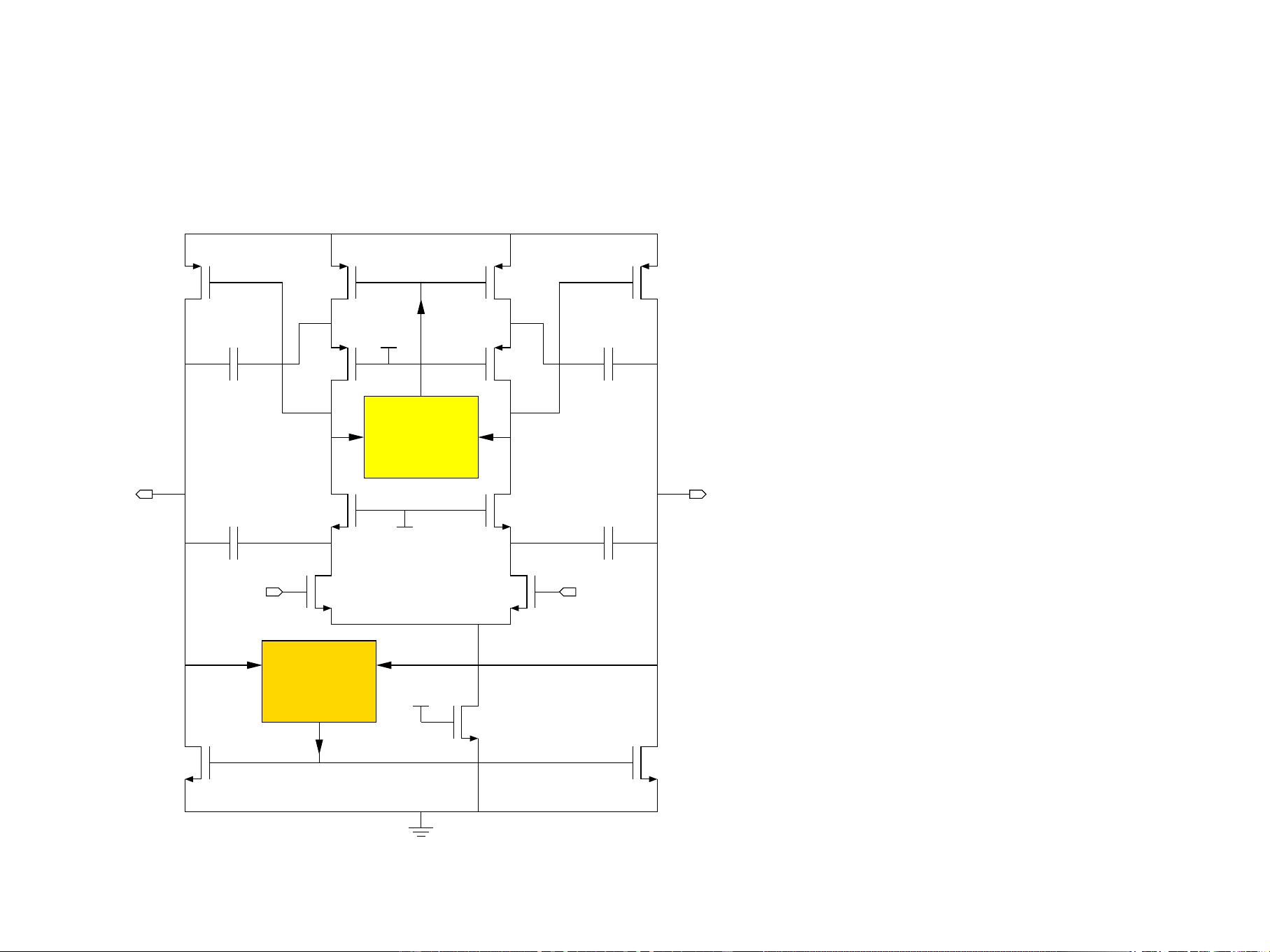
Rail-to-rail output opamp (2 stages)
µs166 V/
CMFB
CT
SC
Vbpc
Vbnc
Vo+ Vo−
Vi+ Vi−
VDD
GND
Cc2
Cc1
Vbn
CMFB
OUTER
INNER
Cc1
Cc2
First stage is a telescopic cascode:
− Shorter channel devices.
− Low Parasitics
− 2 cascode nodes available for
Two Common−Mode−Feedback loops:
− Good stability
− Outer loop is a SC circuit due to
linearity requirements.
− Splitted Compensation Capacitors
gives more Gain−Bandwidth or
Phase−Margin
compensation:
− Large DC gain:
Main Specs:
− Gain−Bandwidth: 200 MHz
− Slew rate: