MMA8451Q
Rev 3, 09/2010
Freescale Semiconductor
Technical Data
An Energy Efficient Solution by Freescale
This document contains certain information on a new product.
Specifications and information herein are subject to change without notice.
© Freescale Semiconductor, Inc., 2010. All rights reserved.
Freescale Semiconductor
Technical Data
An Energy Efficient Solution by Freescale
3-Axis, 14-bit/8-bit
Digital Accelerometer
The MMA8451Q is a smart low-power, three-axis, capacitive micromachined
accelerometer with 14 bits of resolution. This accelerometer is packed with
embedded functions with flexible user programmable options, configurable to two
interrupt pins. Embedded interrupt functions allow for overall power savings
relieving the host processor from continuously polling data. There is access to
both low pass filtered data as well as high pass filtered data, which minimizes the
data analysis required for jolt detection and faster transitions. The device can be
configured to generate inertial wake-up interrupt signals from any combination of
the configurable embedded functions allowing the MMA8451Q to monitor events
and remain in a low power mode during periods of inactivity. The MMA8451Q is
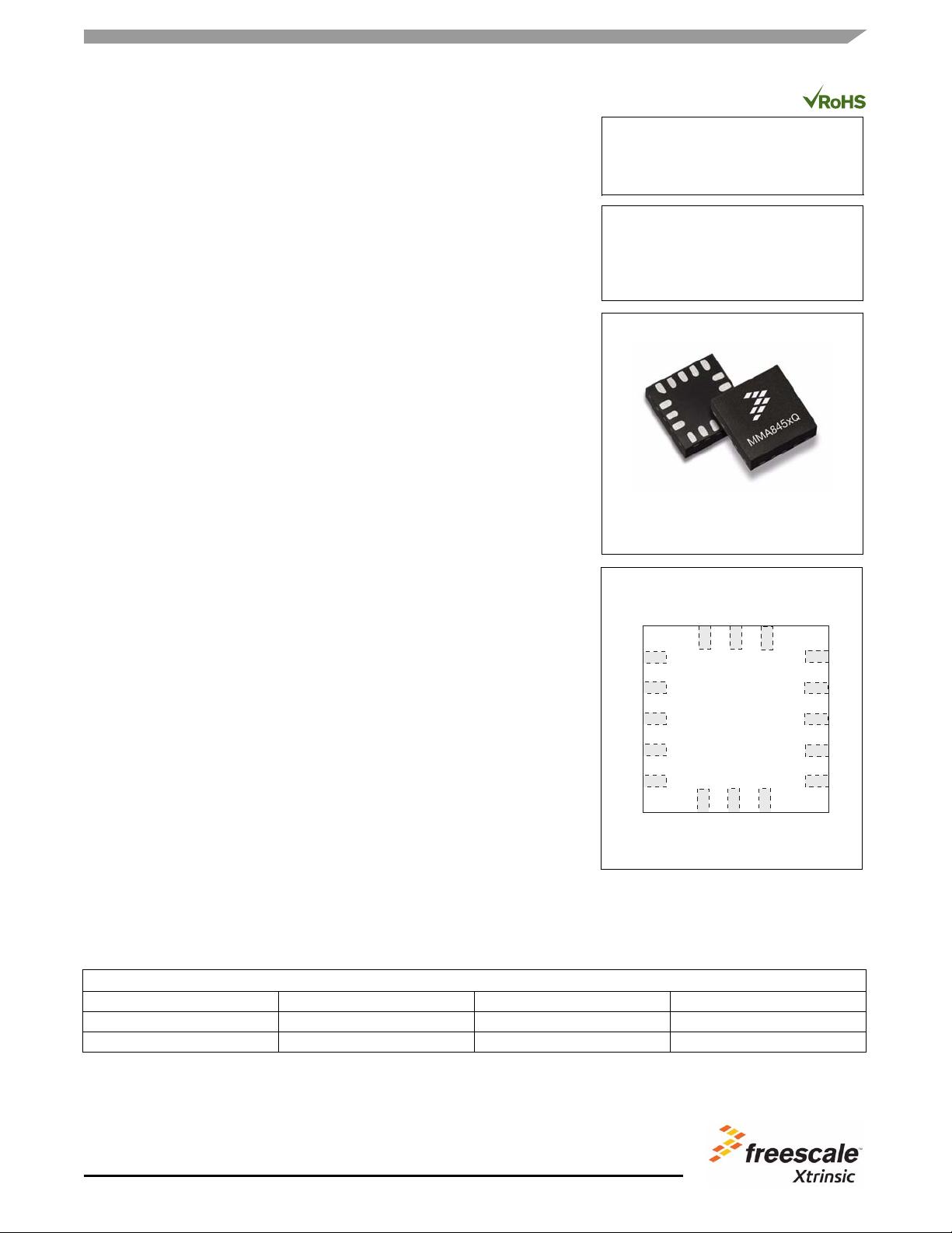
available in a 3 mm x 3 mm x 1 mm QFN package.
Features
• 1.95 V to 3.6 V supply voltage
• 1.6 V to 3.6 V interface voltage
• ±2g/±4g/±8g dynamically selectable full-scale
• Output Data Rates (ODR) from 1.56 Hz to 800 Hz
•99 μg/√Hz noise
• 14-bit and 8-bit digital output
•I
2
C
digital output interface (operates to 2.25 MHz with 4.7 kΩ pull-up
)
• 2 programmable interrupt pins for 7 interrupt sources
• 3 embedded channels of motion detection
– Freefall or Motion Detection: 1 channel
– Pulse Detection: 1 channel
– Jolt Detection: 1 channel
• Orientation (Portrait/Landscape) detection with programmable hysteresis
• Automatic ODR change for Auto-WAKE and return to SLEEP
• 32 sample FIFO
• High Pass Filter Data available per sample and through the FIFO
•Self-Test
• RoHS compliant
• Current Consumption: 6 μA – 165 μA
Typical Applications
• E-Compass applications
• Static orientation detection (Portrait/Landscape, Up/Down, Left/Right, Back/
Front position identification)
• Notebook, E-Reader and Laptop Tumble and Freefall Detection
• Real-time orientation detection (virtual reality and gaming 3D user position
feedback)
• Real-time activity analysis (pedometer step counting, freefall drop detection for HDD, dead-reckoning GPS backup)
• Motion detection for portable product power saving (Auto-SLEEP and Auto-WAKE for cell phone, PDA, GPS, gaming)
• Shock and vibration monitoring (mechatronic compensation, shipping and warranty usage logging)
•
User interface (menu scrolling by orientation change, tap detection for button replacement
)
ORDERING INFORMATION
Part Number Temperature Range Package Description Shipping
MMA8451QT -40°C to +85°C QFN-16 Tray
MMA8451QR1 -40°C to +85°C QFN-16 Tape and Reel
1
GND
VDDIO
SCL
NC
INT2
INT1
GND
GND
SDA
SA0
VDD
NC
NC
NC
BYP
NC
MMA8451Q
2
16
12
13
1415
11
10
3
4
5
6
7
8
9
16 PIN QFN
3 mm x 3 mm x 1 mm
CASE 2077-01
MMA8451Q
MMA8451Q: 3-AXIS DIGITAL
ACCELEROMETER
±2g/±4g/±8g
Top and Bottom View
Top View
Pin Connections

Sensors
2 Freescale Semiconductor
MMA8451Q
Contents
Application Notes for Reference .............................................................................................................................................. 6
1 Block Diagram and Pin Description .................................................................................................................................. 6
1.1 Block Diagram ............................................................................................................................................................. 6
Figure 1. Block Diagram ............................................................................................................................................. 6
1.2 Pin Description ............................................................................................................................................................ 6
Figure 2. Direction of the Detectable Accelerations .................................................................................................... 6
Figure 3. Landscape/Portrait Orientation .................................................................................................................... 7
Figure 4. Application Diagram ..................................................................................................................................... 7
Table 1. Pin Description .............................................................................................................................................. 8
1.3 Soldering Information .................................................................................................................................................. 8
2 Mechanical and Electrical Specifications ......................................................................................................................... 9
2.1 Mechanical Characteristics ......................................................................................................................................... 9
Table 2. Mechanical Characteristics ........................................................................................................................... 9
2.2 Electrical Characteristics ........................................................................................................................................... 10
Table 3. Electrical Characteristics............................................................................................................................. 10
2.3 I
2
C Interface Characteristic ....................................................................................................................................... 11
Table 4. I
2
C Slave Timing Values ............................................................................................................................. 11
Figure 5. I
2
C Slave Timing Diagram ......................................................................................................................... 12
2.4 Absolute Maximum Ratings ...................................................................................................................................... 12
Table 5. Maximum Ratings ....................................................................................................................................... 12
Table 6. ESD and Latch-Up Protection Characteristics ............................................................................................ 12
3 Terminology ...................................................................................................................................................................... 13
3.1 Sensitivity .................................................................................................................................................................. 13
3.2 Zero-g Offset ............................................................................................................................................................. 13
3.3 Self-Test .................................................................................................................................................................... 13
4 Modes of Operation .......................................................................................................................................................... 13
Figure 6. MMA8451Q Mode Transition Diagram ...................................................................................................... 13
Table 7. Mode of Operation Description ................................................................................................................... 13
5 Functionality ...................................................................................................................................................................... 14
5.1 Device Calibration ..................................................................................................................................................... 14
5.2 8-bit or 14-bit Data .................................................................................................................................................... 14
5.3 Internal FIFO Data Buffer .......................................................................................................................................... 14
5.4 Low Power Modes vs. High Resolution Modes ......................................................................................................... 15
5.5 Auto-WAKE/SLEEP Mode ........................................................................................................................................ 15
5.6 Freefall and Motion Detection ................................................................................................................................... 15
5.6.1 Freefall Detection ........................................................................................................................................... 15
5.6.2 Motion Detection ............................................................................................................................................ 15
5.7 Transient Detection ................................................................................................................................................... 16
5.8 Tap Detection ............................................................................................................................................................ 16
5.9 Orientation Detection ................................................................................................................................................ 16
Figure 7. Landscape/Portrait Orientation .................................................................................................................. 16
Figure 8. Illustration of Landscape to Portrait Transition .......................................................................................... 17
Figure 9. Illustration of Portrait to Landscape Transition .......................................................................................... 17
Figure 10. Illustration of Z-Tilt Angle Lockout Transition ........................................................................................... 17
5.10 Interrupt Register Configurations .............................................................................................................................. 18
Figure 11. System Interrupt Generation Block Diagram ........................................................................................... 18
5.11 Serial I
2
C Interface .................................................................................................................................................... 18
Table 8. Serial Interface Pin Description ................................................................................................................... 18
5.11.1 I
2
C Operation ................................................................................................................................................. 19
Table 9. I
2
C Address Selection Table ....................................................................................................................... 19
Single Byte Read ......................................................................................................................................................... 19
Multiple Byte Read ....................................................................................................................................................... 19
Single Byte Write ......................................................................................................................................................... 19
Multiple Byte Write ....................................................................................................................................................... 20
Table 10. I
2
C Device Address Sequence ................................................................................................................. 20
Figure 12. I
2
C Timing Diagram ................................................................................................................................. 20

Sensors
Freescale Semiconductor 3
MMA8451Q
6 Register Descriptions .......................................................................................................................................................21
Table 11. Register Address Map ...............................................................................................................................21
6.1 Data Registers ...........................................................................................................................................................22
F_MODE = 00: 0X00 STATUS: Data Status Register (Read Only) ....................................................................22
Table 12. STATUS Description .................................................................................................................................23
Data Registers: 0x01 OUT_X_MSB, 0x02 OUT_X_LSB, 0x03 OUT_Y_MSB, 0X04 OUT_Y_LSB ............................24
0x01 OUT_X_MSB: X_MSB Register (Read Only) .............................................................................................24
0x02 OUT_X_LSB: X_LSB Register (Read Only) ...............................................................................................24
0x03 OUT_Y_MSB: Y_MSB Register (Read Only) .............................................................................................24
0x04 OUT_Y_LSB: Y_LSB Register (Read Only) ...............................................................................................24
0x05 OUT_Z_MSB: Z_MSB Register (Read Only) .............................................................................................24
0x06 OUT_Z_LSB: Z_LSB Register (Read Only) ...............................................................................................24
6.2 32 Sample FIFO ........................................................................................................................................................24
F_MODE > 0 0x00: F_STATUS FIFO Status Register ................................................................................................24
0x00 F_STATUS: FIFO STATUS Register (Read Only) .....................................................................................24
Table 13. FIFO Flag Event Description .....................................................................................................................25
Table 14. FIFO Sample Count Description ...............................................................................................................25
0x09: F_SETUP FIFO Set-up Register ........................................................................................................................25
0x09 F_SETUP: FIFO Set-up Register (Read/Write) ..........................................................................................25
Table 15. F_SETUP Description ...............................................................................................................................25
0x0A: TRIG_CFG .........................................................................................................................................................26
0x0A: TRIG_CFG Trigger Configuration Register (Read/Write) ..........................................................................26
Table 16. Trigger Configuration Description ..............................................................................................................26
0x0B: SYSMOD System Mode Register ......................................................................................................................26
0x0B SYSMOD: System Mode Register (Read Only) .........................................................................................26
Table 17. SYSMOD Description ................................................................................................................................26
0x0C: INT_SOURCE System Interrupt Status Register ...............................................................................................27
Table 18. INT_SOURCE Description ...............................................................................................
.........................27
0x0D: WHO_AM_I Device ID Register .........................................................................................................................28
0x0D: WHO_AM_I Device ID Register (Read Only) ............................................................................................28
0x0E: XYZ_DATA_CFG Register ................................................................................................................................28
0x0E: XYZ_DATA_CFG (Read/Write) .................................................................................................................28
Table 19. XYZ Data Configuration Descriptions ........................................................................................................28
Table 20. Full Scale Range .......................................................................................................................................28
0x0F: HP_FILTER_CUTOFF High Pass Filter Register ..............................................................................................28
0x0F HP_FILTER_CUTOFF: High Pass Filter Register (Read/Write) ................................................................28
Table 21. High Pass Filter Cut-off Register Descriptions ..........................................................................................28
Table 22. High Pass Filter Cut-off Options ................................................................................................................29
6.3 Portrait/ Landscape Embedded Function Registers ..................................................................................................29
0x10: PL_STATUS Portrait/Landscape Status Register ..............................................................................................29
0x10 PL_STATUS Register (Read Only) ............................................................................................................29
Table 23. PL_STATUS Register Description ............................................................................................................29
0x11 Portrait/Landscape Configuration Register .........................................................................................................30
0x11 PL_CFG Register (Read/Write ...................................................................................................................30
Table 24. PL_CFG Description .................................................................................................................................30
0x12 Portrait/Landscape Debounce Counter ...............................................................................................................30
0x12 PL_COUNT Register (Read/Write) .............................................................................................................30
Table 25. PL_COUNT Description ............................................................................................................................30
Table 26. PL_COUNT Relationship with the ODR ....................................................................................................30
0x13: PL_BF_ZCOMP Back/Front and Z Compensation Register ..............................................................................30
0x13: PL_BF_ZCOMP Register (Read/Write) .....................................................................................................30
Table 27. PL_BF_ZCOMP Description .....................................................................................................................30
Table 28. Z-Lock Threshold Angles ..........................................................................................................................31
Table 29. Back/Front Orientation Definition ..............................................................................................................31
0x14: P_L_THS_REG Portrait/Landscape Threshold and Hysteresis Register ...........................................................31
0x14: P_L_THS_REG Register (Read/Write) ......................................................................................................31
Table 30. P_L_THS_REG Description ......................................................................................................................31
Table 31. Threshold Angle Thresholds Look-up Table .............................................................................................31
Table 32. Trip Angles with Hysteresis for 45° Angle .................................................................................................31

Sensors
4 Freescale Semiconductor
MMA8451Q
6.4 Motion and Freefall Embedded Function Registers .................................................................................................. 32
Mode 1: Freefall Detection with ELE = 0, OAE = 0 ...................................................................................................... 32
Mode 2: Freefall Detection with ELE = 1, OAE = 0 ...................................................................................................... 32
Mode 3: Motion Detection with ELE = 0, OAE = 1 ....................................................................................................... 32
Mode 4: Motion Detection with ELE = 1, OAE = 1 ....................................................................................................... 32
0x15 FF_MT_CFG Freefall/Motion Configuration Register ........................................................................................ 33
0x15 FF_MT_CFG Register (Read/Write) .......................................................................................................... 33
Table 33. FF_MT_CFG Description ......................................................................................................................... 33
Figure 13. FF_MT_CFG High and Low g Level ........................................................................................................ 33
0x16 FF_MT_SRC Freefall/Motion Source Register ................................................................................................... 33
0x16: FF_MT_SRC Freefall and Motion Source Register (Read Only) .............................................................. 33
Table 34. Freefall/Motion Source Description .......................................................................................................... 34
0x17: FF_MT_THS Freefall and Motion Threshold Register ....................................................................................... 34
0x17 FF_MT_THS Register (Read/Write) ........................................................................................................... 34
Table 35. FF_MT_THS Description .......................................................................................................................... 34
0x18 FF_MT_COUNT Debounce Register ................................................................................................................. 35
0x18 FF_MT_COUNT_Register (Read/Write) .................................................................................................... 35
Table 36. FF_MT_COUNT Description ..................................................................................................................... 35
Table 37. FF_MT_COUNT Relationship with the ODR ............................................................................................ 35
Figure 14. DBCNTM Bit Function ............................................................................................................................. 36
6.5 Transient (HPF) Acceleration Detection ................................................................................................................... 37
0x1D: Transient_CFG Register ................................................................................................................................... 37
0x1D TRANSIENT_ CFG Register (Read/Write) ................................................................................................ 37
Table 38. TRANSIENT_ CFG Description ................................................................................................................ 37
0x1E TRANSIENT_SRC Register ............................................................................................................................... 37
0x1E TRANSIENT_SRC Register (Read Only) .................................................................................................. 37
Table 39. TRANSIENT_SRC Description ................................................................................................................. 37
0x1F TRANSIENT_THS Register ................................................................................................................................ 38
0x1F TRANSIENT_THS Register (Read/Write) .................................................................................................. 38
Table 40. TRANSIENT_THS Description ................................................................................................................. 38
0x20 TRANSIENT_COUNT ......................................................................................................................................... 38
0x20 TRANSIENT_COUNT Register (Read/Write) ............................................................................................ 38
Table 41. TRANSIENT_COUNT Description ..........................................................................................
.................. 38
Table 42. TRANSIENT_COUNT Relationship with the ODR .................................................................................... 38
6.6 Single, Double and Directional Tap Detection Registers .......................................................................................... 39
0x21: PULSE_CFG Pulse Configuration Register ....................................................................................................... 39
0x21 PULSE_CFG Register (Read/Write) .......................................................................................................... 39
Table 43. PULSE_CFG Description .......................................................................................................................... 39
0x22: PULSE_SRC Pulse Source Register ................................................................................................................. 39
0x22 PULSE_SRC Register (Read Only) ........................................................................................................... 39
Table 44. PULSE_SRC Description .......................................................................................................................... 39
0x23 - 0x25: PULSE_THSX, Y, Z Pulse Threshold for X, Y & Z Registers ................................................................. 40
0x23 PULSE_THSX Register (Read/Write) ........................................................................................................ 40
Table 45. PULSE_THSX Description ........................................................................................................................ 40
0x24 PULSE_THSY Register (Read/Write) ........................................................................................................ 40
Table 46. PULSE_THSY Description ........................................................................................................................ 40
0x25 PULSE_THSZ Register (Read/Write) ........................................................................................................ 40
Table 47. PULSE_THSZ Description ........................................................................................................................ 40
0x26: PULSE_TMLT Pulse Time Window 1 Register .................................................................................................. 40
0x26 PULSE_TMLT Register (Read/Write) ........................................................................................................ 40
Table 48. PULSE_TMLT Description ........................................................................................................................ 40
Table 49. Time Step for PULSE Time Limit (Reg 0x0F) Pulse_ LPF_EN = 1 .......................................................... 40
Table 50. Time Step for PULSE Time Limit (Reg 0x0F) Pulse_LPF_EN = 0 ........................................................... 41
0x27: PULSE_LTCY Pulse Latency Timer Register .................................................................................................... 41
0x27 PULSE_LTCY Register (Read/Write) ......................................................................................................... 41
Table 51. PULSE_LTCY Description ........................................................................................................................ 41
Table 52. Time Step for PULSE Latency @ ODR and Power Mode (Reg 0x0F) Pulse_ LPF_EN = 1 .................... 41
Table 53. Time Step for PULSE Latency @ ODR and Power Mode (Reg 0x0F) Pulse_ LPF_EN = 0 .................... 41
0x28 PULSE_WIND Register (Read/Write) ................................................................................................................. 42
Table 54. PULSE_WIND Description ........................................................................................................................ 42
Table 55. Time Step for PULSE Detection Window @ ODR and Power Mode (Reg 0x0F) Pulse_ LPF_EN = 1 .... 42
Table 56. Time Step for PULSE Detection Window @ ODR and Power Mode (Reg 0x0F) Pulse_ LPF_EN = 0 ..... 42

Sensors
Freescale Semiconductor 5
MMA8451Q
6.7 Auto-WAKE/SLEEP Detection ..................................................................................................................................43
0x29 ASLP_COUNT Register (Read/Write) ........................................................................................................43
Table 57. ASLP_COUNT Description .......................................................................................................................43
Table 58. ASLP_COUNT Relationship with ODR .....................................................................................................43
Table 59. SLEEP/WAKE Mode Gates and Triggers .................................................................................................43
6.8 Control Registers .......................................................................................................................................................44
0x2A: CTRL_REG1 System Control 1 Register ...........................................................................................................44
0x2A CTRL_REG1 Register (Read/Write) ..........................................................................................................44
Table 60. CTRL_REG1 Description ..........................................................................................................................44
Table 61. SLEEP Mode Rate Description .................................................................................................................44
Table 62. System Output Data Rate Selection ..........................................................................................................44
Table 63. Full Scale Selection ...................................................................................................................................44
0x2B: CTRL_REG2 System Control 2 Register ...........................................................................................................45
0x2B CTRL_REG2 Register (Read/Write) ..........................................................................................................45
Table 64. CTRL_REG2 Description ..........................................................................................................................45
Table 65. MODS Oversampling Modes .....................................................................................................................45
Table 66. MODS Oversampling Modes Current Consumption and Averaging Values at each ODR .......................45
0x2C: CTRL_REG3 Interrupt Control Register ............................................................................................................46
0x2C CTRL_REG3 Register (Read/Write) ..........................................................................................................46
Table 67. CTRL_REG3 Description ..........................................................................................................................46
0x2D: CTRL_REG4 Register (Read/Write) ..................................................................................................................46
0x2D CTRL_REG4 Register (Read/Write) ..........................................................................................................46
Table 68. Interrupt Enable Register Description .......................................................................................................46
0x2E CTRL_REG5 Register (Read/Write) ...................................................................................................................47
0x2E: CTRL_REG5 Interrupt Configuration Register ..........................................................................................47
Table 69. Interrupt Configuration Register Description .............................................................................................47
6.9 User Offset Correction Registers ..............................................................................................................................47
0x2F: OFF_X Offset Correction X Register ..................................................................................................................47
0x2F OFF_X Register (Read/Write) ....................................................................................................................47
Table 70. OFF_X Description ....................................................................................................................................47
0x30: OFF_Y Offset Correction Y Register ..................................................................................................................47
0x30 OFF_Y Register (Read/Write) ....................................................................................................................47
Table 71. OFF_Y Description ....................................................................................................................................47
0x31: OFF_Z Offset Correction Z Register ..................................................................................................................47
0x31 OFF_Z Register (Read/Write) .....................................................................................................................47
Table 72. OFF_Z Description ....................................................................................................................................47
Table 73. MMA8451Q Register Map .........................................................................................................................48
Table 74. Accelerometer Output Data .......................................................................................................................49
Package Dimensions................................................................................................................................................................50