1. Hardware connection of AD9122 Evaluation Board:
(1) SYSCLK (J10) is equal to 1GHz from ADF4351 evaluation board;
(2) The CLKMODESEL (JMP1) is unconnected since PLL is bypassed;
(3) Status Pin S4, S3, S2, S1=1110( Table 8 in datasheet) via JMP7,6,5,4.
(4) VDD_DACDEC (J32) and VDD_DACCLK (J16) need to be connected to 1.8V,
and VDD_DAC3 (J11) need to be connected to 3.3V;
(5) JMP3 need to be connected to external control, which cut off the connection
between USB chip with AD9912 via the 74LVC541A (U4);
(6) JMP2, 8, 9, 10, 11 are useless when we select external control;
(7) Connections between ADuC7026 and AD9912:
ADuC7026
P4.0
P4.1
P4.2
P4.3
GND
AD9912
SCLK
CSB
SDIO
RESET
GND
P1 connector
(8) Both COMS output and HSTL output are power-down.
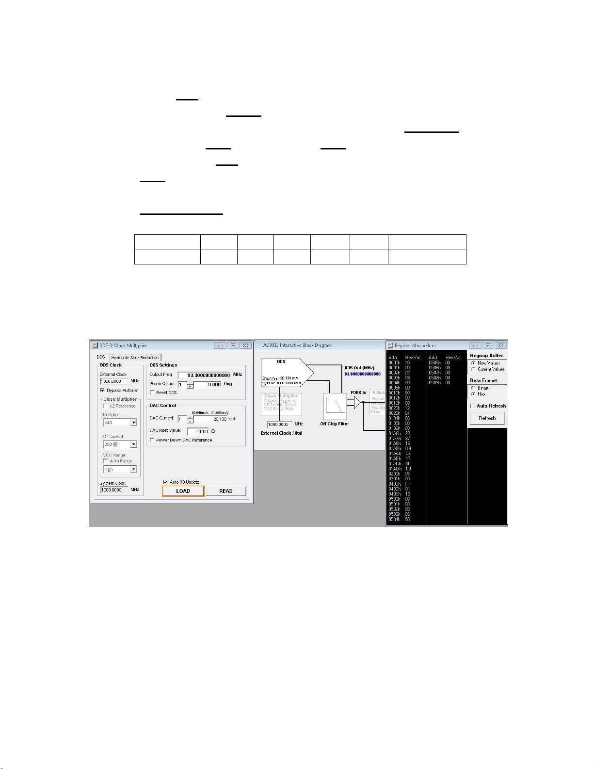
(9) The output frequency of DDS is 93MHz.
2. According to the conditions above, we can get the value of registers by using of
the evaluation board software.
3. The only thing we need to do is transferring the data to the registers via SPI, the
Timing diagram are shown as the page 29 of the datasheet.
In the code, we make use of three writing functions to transfer the data.
The practical tests timing of the functions are shown as below:
(1) MSB First, 16-bit Instruction, One Byte. (Y: CS, G: SCLK, R: SDIO)
The 24-bit data is 0x137018 (just for example)


