没有合适的资源?快使用搜索试试~ 我知道了~
BL24C256超高性价比EEPOM,SOIC8,TSSOP8两种封装都有。-BL24C256A.PDF
需积分: 21 4 下载量 25 浏览量
2019-09-03
10:55:10
上传
评论 2
收藏 548KB PDF 举报
温馨提示
BL24C256超高性价比EEPOM,SOIC8,TSSOP8两种封装都有。-BL24C256A.PDF
资源推荐
资源详情
资源评论

BL24C256A 256Kbits (32768×8)
BL24C256A 256Kbits (32768×8) Belling Proprietary Information. Unauthorized Photocopy and Duplication Prohibited
© 2016 Belling All Rights Reserved www.belling.com.cn
1-18
Features
Compatible with all I
2
C bidirectional data
transfer protocol
Memory array:
– 256 Kbits (32 Kbytes) of EEPROM
– Page size: 64 bytes
– Additional Write lockable page
Single supply voltage and high speed:
– 1 MHz (2.5V)
– 400 KHz(1.7V)
– 100 KHz(1.7V)
Random and sequential Read modes
Write:
– Byte Write within 3 ms
– Page Write within 3 ms
– Partial Page Writes Allowed
Write Protect Pin for Hardware Data Protection
Schmitt Trigger, Filtered Inputs for Noise
Suppression
High-reliability
– Endurance: 1 Million Write Cycles
– Data Retention: 100 Years
Enhanced ESD/Latch-up protection
– HBM 8000V
8-lead PDIP/SOP/TSSOP/UDFN and WLCSP4
packages
Description
The BL24C256A provides 262144 bits of serial
electrically erasable and programmable read-
only memory (EEPROM), organized as 32768
words of 8 bits each.
The device is optimized for use in many
industrial and commercial applications where
low-power and low-voltage operation are
essential.
The BL24C256A offers an additional page,
named the Identification Page (64 bytes). The
Identification Page can be used to store
sensitive application parameters which can be
(later) permanently locked in Read-only mode.
Pin Configuration
A0
A1
A2
GND
VCC
WP
A0
A1
A2
GND
A0
A1
A2
GND
A0
A1
A2
GND
VCC
WP
VCC
WP
VCC
WP
1
2
3
4
5
6
7
8
1
2
3
4
1
2
3
4
5
6
7
8
5
6
7
8
5
6
7
8
1
2
3
4
8-lead PDIP 8-lead SOP 8-lead TSSOP 8-pad DFN
1 2
A
B
Vcc
Vss
SCL
SDA
WLCSP4
Bottem view
Marking side
(top view)
SCL
SDA
SCL
SDA
SCL
SDA
SCL
SDA

BL24C256A 256Kbits (32768×8)
BL24C256A 256Kbits (32768×8) Belling Proprietary Information. Unauthorized Photocopy and Duplication Prohibited
© 2016 Belling All Rights Reserved www.belling.com.cn
2-18
Pin Descriptions
Pin Name Type Functions
A0-A2 I Address Inputs
SDA I/O Serial Data
SCL I Serial Clock Input
WP I Write Protect
GND P Ground
Vcc P Power Supply
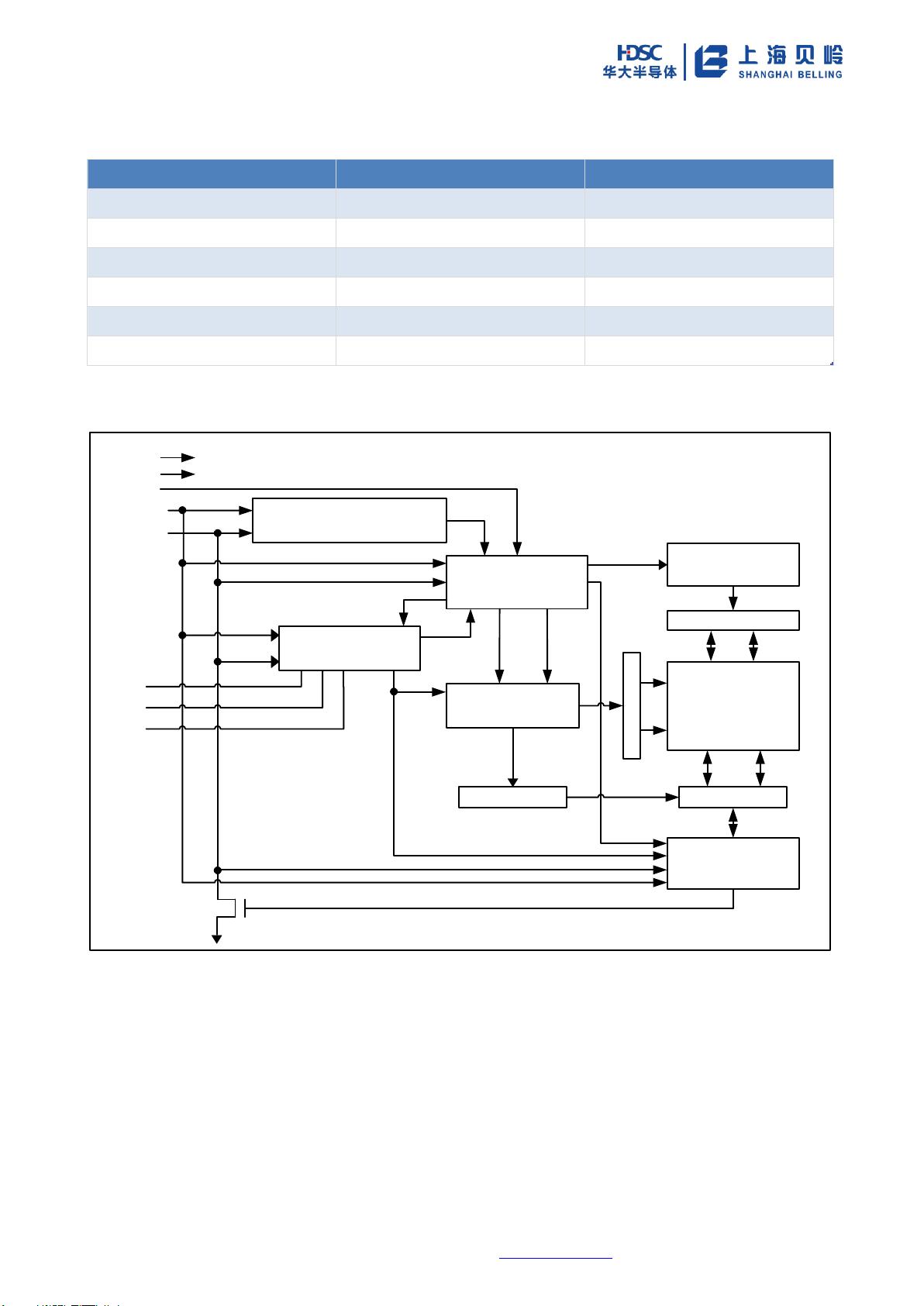
Block Diagram
START STOP
LOGIC
SERIAL CONTROL
LOGIC
SCL
SDA
GND
Vcc
DEVICE ADDRESS
COMPARATOR
LOAD
CCMP
DATA WORD
ADRESS COUNTER
LOAD INC
X DECODER
Y DECODER SERIAL MUX
EEPROM
EN
DATA RECOVERY
HIGH VOLTAGE
PUMP/TIMING
DOUT/ACKNOWLEDGE
DIN
DOUT
A0
A1
A2
WP
DEVICE/PAGE ADDRESSES (A2, A1 and A0): The A2, A1 and A0 pins are device address inputs that are hard
wire for the BL24C256A. Eight 256K devices may be addressed on a single bus system (device
addressing is discussed in detail under the Device Addressing section).
SERIAL DATA (SDA): The SDA pin is bi-directional for serial data transfer. This pin is open-drain driven
and may be wire-ORed with any number of other open-drain or open- collector devices.
SERIAL CLOCK (SCL): The SCL input is used to positive edge clock data into each EEPROM device
and negative edge clock data out of each device.

BL24C256A 256Kbits (32768×8)
BL24C256A 256Kbits (32768×8) Belling Proprietary Information. Unauthorized Photocopy and Duplication Prohibited
© 2016 Belling All Rights Reserved www.belling.com.cn
3-18
WRITE PROTECT (WP): The BL24C256A has a Write Protect pin that provides hardware data protection.
The Write Protect pin allows normal read/write operations when connected to ground (GND). When
the Write Protection pin is connected to Vcc, the write protection feature is enabled and operates as
shown in the following Table 2.
WP Pin Status BL24C256A
At VCC Full(256K)Array
At GND Normal Read/Write Operations
Functional Description
1. Memory Organization
BL24C256A, 256K SERIAL EEPROM: Internally organized with 256 pages of 64 bytes each, the 256K
requires a 15-bit data word address for random word addressing.
2. Device Operation
CLOCK and DATA TRANSITIONS: The SDA pin is normally pulled high with an external device. Data on the
SDA pin may change only during SCL low time periods (see Figure 2). Data changes during SCL high
periods will indicate a start or stop condition as defined below.
START CONDITION: A high-to-low transition of SDA with SCL high is a start condition which must
precede any other command (see Figure 3).
STOP CONDITION: A low-to-high transition of SDA with SCL high is a stop condition. After a read
sequence, the stop command will place the EEPROM in a standby power mode (see Figure 3).
ACKNOWLEDGE: All addresses and data words are serially transmitted to and from the EEPROM in 8-bit
words. The EEPROM sends a "0" to acknowledge that it has received each word. This happens during
the ninth clock cycle.
STANDBY MODE: The BL24C256A features a low-power standby mode which is enabled: (a) upon power-
up and (b) after the receipt of the STOP bit and the completion of any internal operations.
MEMORY RESET: After an interruption in protocol, power loss or system reset, any two-wire part can be
reset by following these steps:
1. Clock up to 9 cycles.
2. Look for SDA high in each cycle while SCL is high.
3. Create a start condition.
剩余17页未读,继续阅读
资源评论

weixin_38744435
- 粉丝: 373
- 资源: 2万+
上传资源 快速赚钱
 我的内容管理
展开
 我的资源
快来上传第一个资源
 我的收益 登录查看自己的收益
 我的积分
登录查看自己的积分
 我的C币
登录后查看C币余额
 我的收藏
我的收藏  我的下载
我的下载  下载帮助
下载帮助

 前往需求广场,查看用户热搜
最新资源
- common.war
- shia.war
- 长沙理工大学大物实验-霍尔效应数据处理
- 基于C语言的医院叫号系统-叫号页面大屏.zip
- Thinkphp运营工商资质注册办理类企业网站模板+前后端源码
- 蒜苔采摘机sw16可编辑全套技术开发资料100%好用.zip
- 佳能c3125 c3120 维修手册
- springboot+MySQL+vue汽车租赁智慧管理96317
- Java编程练习题集锦-涵盖基础算法与实际应用案例
- 基于 Vision Transformer 网络对细胞图像的多类别识别项目【包含完整数据集、代码等】
- Code of Conduct on Energy Consumption of Broadband Equipment
- 十字型声子晶体案例三相PWM逆变器闭环仿真,电压电流双闭环控制 在0.2s时突加负载测试系统抗扰性 模型中包含主电路,坐标变,电压电流双环PI控制器,SVPWM控制,PWM发生器 matlab s
- 卡尔曼滤波算法 二阶电池等效电路模型
- c#开发,通过短信猫发送短信的demo
- 基于MobileViT的xxs、xs、s版本实现的汽车轮胎缺陷图像识别迁移学习分类实战【包含数据集+完整代码】
- 五相电机simulink,五相永磁同步电机simulink,PI双闭环SVPWM矢量控制,分十个扇区,波形良好,动态相应能力强,矢量控制,模型很复杂
资源上传下载、课程学习等过程中有任何疑问或建议,欢迎提出宝贵意见哦~我们会及时处理!
点击此处反馈


安全验证
文档复制为VIP权益,开通VIP直接复制
 信息提交成功