没有合适的资源?快使用搜索试试~ 我知道了~
通过调制施加电压在ap-Cu2ZnSnS4 / n-GaN异质结光电二极管中的替代光谱光响应
1 下载量 85 浏览量
2021-03-18
19:48:37
上传
评论
收藏 376KB PDF 举报
温馨提示
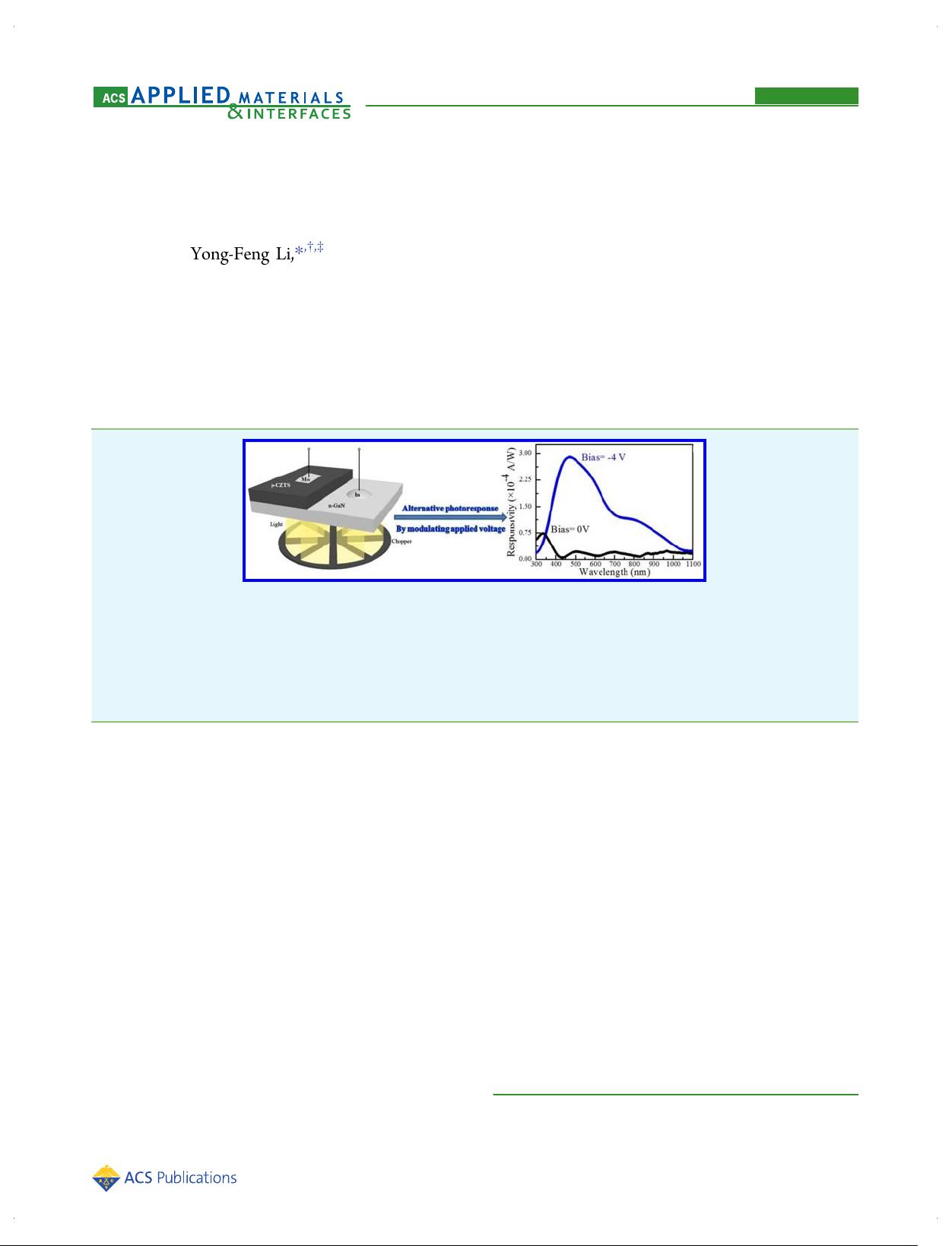
我们报告p-Cu2ZnSnS4(p-CZTS)/ n-GaN异质结光电二极管中的替代可见光和紫外光响应光谱。使用磁控溅射法将CZTS膜沉积在n-GaN /蓝宝石衬底上。 p-CZTS / n-GaN异质结光电二极管的电流-电压特性显示出良好的整流性能。这光谱响应测量表明,可以通过施加零偏和反向偏压将光电二极管的响应波长从紫外线调谐到可见光区域。提出了在p-CZTS / n-GaN异质结界面处的能带对准来解释器件的光谱响应。
资源推荐
资源详情
资源评论

Alternative Spectral Photoresponse in a p‑Cu
2
ZnSnS
4
/n‑GaN
Heterojunction Photodiode by Modulating Applied Voltage
Gang Yang,
†
Yong-Feng Li,*
,†,‡
Bin Yao,*
,†,‡
Zhan-Hui Ding,
†
Rui Deng,
§
Xuan Fang,
∥
and Zhi-Peng Wei
∥
†
State Key Lab of Superhard Materials and College of Physics, Jilin University, Changchun 130012, People’s Republic of China
‡
Key Laboratory of Physics and Technology for Advanced Batteries (Ministry of Education), College of Physics, Jilin University,
Changchun 130012, China
§
School of Materials Science and Engineering, Changchun University of Science and Technology, Changchun 130022, China
∥
State Key Laboratory on High-Power Semiconductor Lasers, Changchun University of Science and Technology, 7186 Wei-Xing
Road, Changchun 130022, China
ABSTRACT: We report alternative visible and ultraviolet light response spectra in a p-Cu
2
ZnSnS
4
(p-CZTS)/n-GaN
heterojunction photodiode. A CZTS film was deposited on an n-GaN/sapphire substrate using a magnetron sputtering method.
Current−voltage characteristic of the p-CZTS/n-GaN heterojunction photodiode showed a good rectifying behavior. The
spectral response measurements indicate that the response wavelength of the photodiode can be tuned from ultraviolet to visible
regions via applying zero and reverse bias. A band alignment at the interface of the p-CZTS/n-GaN heterojunction was proposed
to interpret the spectral response of the device.
KEYWORDS: photodiode, GaN, magnetron sputtering, Cu
2
ZnSnS
4
, heterojunction
■
INTRODUCTION
Solar energy is considered to be the most economic and
effective available renewable energy resources.
1−3
Photovoltaic
(PV) cells including thin film solar cells,
4
dye-sensitized solar
cells,
5
organic bulk junction solar cells,
6
and hybrid perovskite
solar cells
7,8
have been widely investigated because they can
convert sunlight directly into electricity. In recent years, the
kesterite Cu
2
ZnSnS
4
(CZTS) emerged as a potential p-type
material used in thin film photovoltaic applications.
9−12
It has
an ideal direct bandgap of about 1.5 eV and a large absorption
coefficient (>10
4
cm
−1
).
13,14
The use of only nontoxic and
abundant elements makes it to be more environmental friendly
and economical compared with CdTe and Cu(In
1−x
Ga
x
)-
Se
2.
15,16
Recently, various deposition techniques including
vacuum and nonvacuum methods were applied to fabricate
CZTS solar cells, and the power conversion efficiency (PCE)
record has been updated rapidly.
17−19
A typical structure of CZTS solar cells is Mo/CZTS/CdS/
ZnO/ZnO:Al/Al.
11
The n-type CdS buffer layer is fabricated
on the p-type CZTS absorption layer to form a p−n junction,
where carriers are separated as light irradiates. The wide
bandgap semiconductors including an intrinsic ZnO and a
heavily n-doped ZnO:Al were usually used as the window layer,
which reduces the series resistance of solar cells.
20
Recently,
researches also focused on direct deposition of n-type wide-
bandgap ZnO on p-type CZTS to form Cd-free p-CZTS/n-
ZnO heterojunction devices.
21,22
Htay et al. reported the higher
open circuit voltage (V
oc
) and relative quantum efficiency at the
short wavelength regions in the p-CZTS/n-ZnO heterojunction
solar cells than those using CdS as the buffer layer.
23
They
ascribed these to the higher built-in potential induced by the
wider bandgap ZnO and the increase of transparency. In
addition, the proposed type-I band alignment of CZTS/ZnO
heterojunction (i.e., the conduction band of CZTS is lower
than that of ZnO) can reduce the recombination rate greatly.
Among lots of wide-bandgap semiconductors, gallium nitride
(GaN) has the same wurtzite structure with ZnO and similar
wide direct bandgap (3.4 eV).
24,25
But few reports were
available for the CZTS/GaN heterojunction. Due to the
advantages of high saturation velocity (2.7 × 10
7
cm/s),
radiation hardness, tolerability of aggressive environments, and
a more mature processing technique, GaN was widely used for
fabricating photodetectors.
26−28
More importantly, the type-I
band alignment of the CZTS/GaN interface with a small
Received: May 17, 2015
Accepted: July 16, 2015
Published: July 16, 2015
Research Article
www.acsami.org
© 2015 American Chemical Society 16653 DOI: 10.1021/acsami.5b04287
ACS Appl. Mater. Interfaces 2015, 7, 16653−16658
资源评论

weixin_38590685
- 粉丝: 3
- 资源: 920
上传资源 快速赚钱
 我的内容管理
展开
 我的资源
快来上传第一个资源
 我的收益 登录查看自己的收益
 我的积分
登录查看自己的积分
 我的C币
登录后查看C币余额
 我的收藏
我的收藏  我的下载
我的下载  下载帮助
下载帮助

 前往需求广场,查看用户热搜
最新资源
- 计算机二级考试全面备考指南与学习心得
- 树木的信息数据集(德国罗斯托克地区树木的信息)
- Python爬虫基础知识与实践指南
- 连接ESP32手表来做验证20241223-140953.pcapng
- 有源电力滤波器,APF,有源电力滤波器仿真,电力电子仿真,无差拿控制,谐波补偿 提供参考文献
- 某平台广告投入分析与销售预测
- 国际象棋桌子检测6-YOLO(v5至v9)、COCO、CreateML、Darknet、Paligemma、TFRecord数据集合集.rar
- 永磁同步电机参数辨识模型,在线辨识,离线辨识,电参数机械参数均可辨识,基于最小二乘法,滑模观测,电压注入,模型参考自适应等 机械参数在线 离线 ,电气参数在线 (三种方法,最小二乘和mras以及卡尔
- dbeaver-ce-24.3.1-x86-64-setup.exe
- 基于粒子群的ieee30节点优化、配电网有功-无功优化 软件:Matlab+Matpowre 介绍:对配电网中有功-无功协调优化调度展开研究,通过对光伏电源、储能装置、无功电源和变压器分接头等设备协调
- 基于ssm的高校教务管理系统设计与实现
- VirtualGL-2.6.5.x86-64.rpm
- 艾利和iriver Astell&Kern SP3000 V1.30升级固件
- turbovnc-2.2.6.x86-64.rpm
- Labview Modbus-Tcp和西门子全糸列pLC通讯所有数据类型均能读写,速度快,使用在多个项目上,运行稳定,可以扩展到其它品牌PLc,上位机程序一样,只是PLC程序稍微变动一下,上下位机源
- 国际象棋检测10-YOLO(v5至v11)、COCO、CreateML、Paligemma、TFRecord、VOC数据集合集.rar
资源上传下载、课程学习等过程中有任何疑问或建议,欢迎提出宝贵意见哦~我们会及时处理!
点击此处反馈


安全验证
文档复制为VIP权益,开通VIP直接复制
 信息提交成功