没有合适的资源?快使用搜索试试~ 我知道了~
触摸控制器tsc20464
需积分: 0 0 下载量 87 浏览量
2022-08-04
15:43:37
上传
评论
收藏 791KB PDF 举报
温馨提示
试读
32页
触摸控制器tsc20464
资源详情
资源评论
资源推荐
FEATURES
D SAME PINOUT AS ADS7846
D 2.2V TO 5.25V OPERATION
D 1.5V TO 5.25V DIGITAL I/O
D INTERNAL 2.5V REFERENCE
D DIRECT BATTERY MEASUREMENT (0V TO 6V)
D ON-CHIP TEMPERATURE MEASUREMENT
D TOUCH-PRESSURE MEASUREMENT
D QSPI AND SPI 3-WIRE INTERFACE
D AUTO POWER-DOWN
D AVAILABLE IN TSSOP-16, QFN-16, AND
VFBGA-48 PACKAGES
APPLICATIONS
D PERSONAL DIGITAL ASSISTANTS
D PORTABLE INSTRUMENTS
D POINT-OF-SALE TERMINALS
D PAGERS
D TOUCH SCREEN MONITORS
D CELLULAR PHONES
US Patent No. 6246394
QSPI and SPI are registered trademarks of Motorola.
DESCRIPTION
The TSC2046 is a next-generation version to the
ADS7846 4-wire touch screen controller which supports
a low-voltage I/O interface from 1.5V to 5.25V. The
TSC2046 is 100% pin-compatible with the existing
ADS7846, and will drop into the same socket. This allows
for easy upgrade of current applications to the new
version. The TSC2046 also has an on-chip 2.5V
reference that can be used for the auxiliary input, battery
monitor, and temperature measurement modes. The
reference can also be powered down when not used to
conserve power. The internal reference operates down to
2.7V supply voltage, while monitoring the battery voltage
from 0V to 6V.
The low-power consumption of < 0.75mW typ at 2.7V
(reference off), high-speed (up to 125kHz sample rate),
and on-chip drivers make the TSC2046 an ideal choice for
battery-operated systems such as personal digital
assistants (PDAs) with resistive touch screens, pagers,
cellular phones, and other portable equipment. The
TSC2046 is available in TSSOP-16, QFN-16, and
VFBGA-48 packages and is specified over the –40°C to
+85°C temperature range.
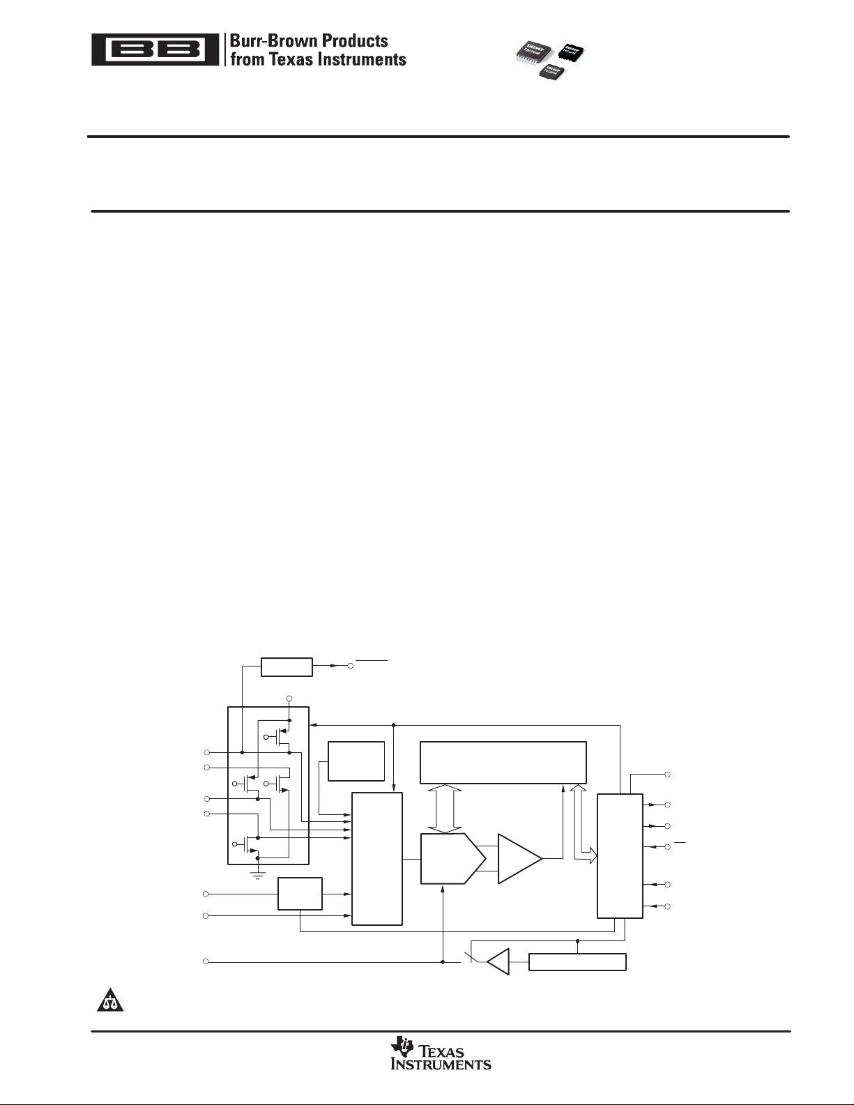
CDAC
Internal 2.5V Reference
SAR
TSC2046
Comparator
6− Channel
MUX
Serial
Data
In/Out
Temperature
Sensor
Pen Detect
Battery
Monitor
DOUT
BUSY
CS
DCLK
DIN
V
BAT
AUX
V
REF
+V
CC
IOVDD
X+
X−
Y+
Y
−
PENIRQ
TSC2046
SBAS265F − OCTOBER 2002 − REVISED AUGUST 2007
Low Voltage I/O
TOUCH SCREEN CONTROLLER
! !
www.ti.com
Copyright 2002−2007, Texas Instruments Incorporated
All trademarks are the property of their respective owners.
Please be aware that an important notice concerning availability, standard warranty, and use in critical applications of Texas Instruments
semiconductor products and disclaimers thereto appears at the end of this data sheet.
"#$%&
SBAS265F − OCTOBER 2002 − REVISED AUGUST 2007
www.ti.com
2
ABSOLUTE MAXIMUM RATINGS
(1)
+V
CC
and IOVDD to GND −0.3V to +6V. . . . . . . . . . . . . . . . . . . . .
Analog Inputs to GND −0.3V to +V
CC
+ 0.3V. . . . . . . . . . . . . . . . .
Digital Inputs to GND −0.3V to IOVDD + 0.3V. . . . . . . . . . . . . . . . .
Power Dissipation 250mW. . . . . . . . . . . . . . . . . . . . . . . . . . . . . . . . .
Maximum Junction Temperature +150°C. . . . . . . . . . . . . . . . . . . . . .
Operating Temperature Range −40°C to +85°C. . . . . . . . . . . . . . . .
Storage Temperature Range −65°C to +150°C. . . . . . . . . . . . . . . . .
Lead Temperature (soldering, 10s) +300°C. . . . . . . . . . . . . . . . . . . . .
(1)
Stresses above these ratings may cause permanent damage.
Exposure to absolute maximum conditions for extended periods
may degrade device reliability. These are stress ratings only, and
functional operation of the device at these or any other conditions
beyond those specified is not implied.
ELECTROSTATIC DISCHARGE SENSITIVITY
This integrated circuit can be damaged by ESD. Texas
Instruments recommends that all integrated circuits be
handled with appropriate precautions. Failure to observe
proper handling and installation procedures can cause damage.
ESD damage can range from subtle performance degradation to
complete device failure. Precision integrated circuits may be more
susceptible to damage because very small parametric changes could
cause the device not to meet its published specifications.
PACKAGE/ORDERING INFORMATION
(1)
PRODUCT
NOMINAL
PENIRQ
PULLUP
RESISTOR
VALUES
MAXIMUM
INTEGRAL
LINEARITY
ERROR
(LSB)
PACKAGE-
LEAD
PACKAGE
DESIGNATOR
SPECIFIED
TEMPERATURE
RANGE
PACKAGE
MARKING
ORDERING
NUMBER
TRANSPORT
MEDIA, QUANTITY
TSSOP-16
PW
−40°C to +85°C
TSC2046I
TSC2046IPW Rails, 100
TSSOP-16 PW −40°C to +85°C TSC2046I
TSC2046IPWR Tape and Reel, 2500
4x4, 1mm
TSC2046IRGVT Tape and Reel, 250
TSC2046I
50kΩ
±2
4x4, 1mm
QFN-16
RGV −40°C to +85°C TSC2046
TSC2046IRGVR Tape and Reel, 2500
TSC2046I 50kΩ ±2
QFN-16
RGV
−40 C to +85 C
TSC2046
TSC2046IRGVRG4 Tape and Reel, 2500
4x4
GQC −40°C to +85°C AZ2046 TSC2046IGQCR Tape and Reel, 2500
4x4
VFBGA-48
ZQC
−40°C to +85°C
BC2046
TSC2046IZQCT Tape and Reel, 250
VFBGA-48
ZQC −40°C to +85°C BC2046
TSC2046IZQCR Tape and Reel, 2500
TSC2046I
(2)
90kΩ
±2
4x4
GQC −40°C to +85°C AZ2046A TSC2046IGQCR-90 Tape and Reel, 2500
TSC2046I
(2)
90kΩ ±2
4x4
VFBGA-48
ZQC −40°C to +85°C BC2046A TSC2046IZQCR-90 Tape and Reel, 2500
(1)
For the most current package and ordering information, see the Package Option Addendum located at the end of this data sheet, or see the TI web
site at www.ti.com.
(2)
High-impedance version.
"#$%&
SBAS265F − OCTOBER 2002 − REVISED AUGUST 2007
www.ti.com
3
ELECTRICAL CHARACTERISTICS: V
S
= +2.7V to +5.5V
At T
A
= −40°C to +85°C, +V
CC
= +2.7V, V
REF
= 2.5V internal voltage, f
SAMPLE
= 125kHz, f
CLK
= 16 • f
SAMPLE
= 2MHz, 12-bit mode, digital
inputs = GND or IOVDD, and +V
CC
must be • IOVDD, unless otherwise noted.
TSC2046
PARAMETER CONDITION MIN TYP MAX UNITS
ANALOG INPUT
Full-Scale Input Span Positive Input−Negative Input 0 V
REF
V
Absolute Input Range Positive Input −0.2 +V
CC
+ 0.2 V
Negative Input −0.2 +0.2 V
Capacitance 25 pF
Leakage Current 0.1 µA
SYSTEM PERFORMANCE
Resolution 12 Bits
No Missing Codes 11 Bits
Integral Linearity Error ±2 LSB
(1)
Offset Error ±6 LSB
Gain Error External V
REF
±4 LSB
Noise Including Internal V
REF
70 µVrms
Power-Supply Rejection 70 dB
SAMPLING DYNAMICS
Conversion Time 12 CLK Cycles
Acquisition Time 3 CLK Cycles
Throughput Rate 125 kHz
Multiplexer Settling Time 500 ns
Aperture Delay 30 ns
Aperture Jitter 100 ps
Channel-to-Channel Isolation V
IN
= 2.5V
PP
at 50kHz 100 dB
SWITCH DRIVERS
On-Resistance
Y+, X+ 5 Ω
Y−, X− 6 Ω
Drive Current
(2)
Duration 100ms 50 mA
REFERENCE OUTPUT
Internal Reference Voltage 2.45 2.50 2.55 V
Internal Reference Drift 15 ppm/°C
Quiescent Current 500 µA
REFERENCE INPUT
Range 1.0 +V
CC
V
Input Impedance SER/DFR = 0, PD1 = 0 1 GΩ
Internal Reference Off
Internal Reference On 250 Ω
BATTERY MONITOR
Input Voltage Range 0.5 6.0 V
Input Impedance
Sampling Battery 10 kΩ
Battery Monitor Off 1 GΩ
Accuracy V
BAT
= 0.5V to 5.5V, External V
REF
= 2.5V −2 +2 %
V
BAT
= 0.5V to 5.5V, Internal Reference −3 +3 %
TEMPERATURE MEASUREMENT
Temperature Range −40 +85 °C
Resolution Differential Method
(3)
1.6 °C
TEMP0
(4)
0.3 °C
Accuracy Differential Method
(3)
±2 °C
TEMP0
(4)
±3 °C
(1)
LSB means Least Significant Bit. With V
REF
= +2.5V, one LSB is 610µV.
(2)
Assured by design, but not tested. Exceeding 50mA source current may result in device degradation.
(3)
Difference between TEMP0 and TEMP1 measurement, no calibration necessary.
(4)
Temperature drift is −2.1mV/°C.
(5)
TSC2046 operates down to 2.2V.
(6)
IOVDD must be − (+V
CC
).
(7)
Combined supply current from +V
CC
and IOVDD. Typical values obtained from conversions on AUX input with PD0 = 0.
"#$%&
SBAS265F − OCTOBER 2002 − REVISED AUGUST 2007
www.ti.com
4
ELECTRICAL CHARACTERISTICS: V
S
= +2.7V to +5.5V (continued)
At T
A
= −40°C to +85°C, +V
CC
= +2.7V, V
REF
= 2.5V internal voltage, f
SAMPLE
= 125kHz, f
CLK
= 16 • f
SAMPLE
= 2MHz, 12-bit mode, digital
inputs = GND or IOVDD, and +V
CC
must be • IOVDD, unless otherwise noted.
TSC2046
PARAMETER UNITSMAXTYPMINCONDITION
DIGITAL INPUT/OUTPUT
Logic Family CMOS
Capacitance All Digital Control Input Pins 5 15 pF
V
IH
| I
IH
| ≤ +5µA IOVDD • 0.7 IOVDD + 0.3 V
V
IL
| I
IL
| ≤ +5µA −0.3 0.3 • IOVDD V
V
OH
I
OH
= −250µA IOVDD • 0.8 V
V
OL
I
OL
= 250µA 0.4 V
Data Format
Straight
Binary
POWER-SUPPLY REQUIREMENTS
+V
CC
(5)
Specified Performance 2.7 3.6 V
Operating Range 2.2 5.25 V
IOVDD
(6)
1.5 +V
CC
V
Quiescent Current
(7)
Internal Reference Off 280 650 µA
Internal Reference On 780 µA
f
SAMPLE
= 12.5kHz 220 µA
Power-Down Mode with 3 µA
CS = DCLK = DIN = IOVDD
Power Dissipation +V
CC
= +2.7V 1.8 mW
TEMPERATURE RANGE
Specified Performance −40 +85 °C
(1)
LSB means Least Significant Bit. With V
REF
= +2.5V, one LSB is 610µV.
(2)
Assured by design, but not tested. Exceeding 50mA source current may result in device degradation.
(3)
Difference between TEMP0 and TEMP1 measurement, no calibration necessary.
(4)
Temperature drift is −2.1mV/°C.
(5)
TSC2046 operates down to 2.2V.
(6)
IOVDD must be − (+V
CC
).
(7)
Combined supply current from +V
CC
and IOVDD. Typical values obtained from conversions on AUX input with PD0 = 0.
"#$%&
SBAS265F − OCTOBER 2002 − REVISED AUGUST 2007
www.ti.com
5
PIN CONFIGURATION
Top View
1
2
3
4
5
6
7
8
+V
CC
X+
Y+
X
−
Y
−
GND
V
BAT
AUX
DCLK
CS
DIN
BUSY
DOUT
PENIRQ
IOVDD
V
REF
16
15
14
13
12
11
10
9
TSC2046
Top View QFN
TSSOP
Top View VFBGA
NC
NC
A
B
C
D
E
F
G
21 3 4 5 6 7
DCLK
+V
CC
+V
CC
X+
Y+
PENIRQ
IOVDD
V
REF
AUX
CS DIN BUSY DOUT
X
−
Y
−
GND GND V
BAT
NC
NC
NC
NC
NC
NC
NC
NC
NC
NC
NC
NC
NC
NC
NC
NC
NC
NC
NC
NC NC
NC
NC
NC
NC
NCNC
NC
BUSY
DIN
CS
DCLK
AUX
V
BAT
GND
Y
−
1
2
3
4
12
11
10
9
TSC2046
DOUT
PENIRQ
IOVDD
V
REF
16
15
14
13
+V
CC
X+
Y+
X
−
5
6
7
8
(1)
The thermal pad is internally connected to the substrate. This pad can be connected to the analog ground or left floating. Keep the thermal
pad separate from the digital ground, if possible.
(Thermal Pad)
(1)
PIN DESCRIPTION
TSSOP PIN # VFBGA PIN # QFN PIN # NAME DESCRIPTION
1 B1 and C1 5 +V
CC
Power Supply
2 D1 6 X+ X+ Position Input
3 E1 7 Y+ Y+ Position Input
4 G2 8 X− X− Position Input
5 G3 9 Y− Y− Position Input
6 G4 and G5 10 GND Ground
7 G6 11 V
BAT
Battery Monitor Input
8 E7 12 AUX Auxiliary Input to ADC
9 D7 13 V
REF
Voltage Reference Input/Output
10 C7 14 IOVDD Digital I/O Power Supply
11 B7 15 PENIRQ Pen Interrupt
12 A6 16 DOUT
Serial Data Output. Data is shifted on the falling edge of DCLK. This output is high
impedance when CS
is high.
13 A5 1 BUSY Busy Output. This output is high impedance when CS is high.
14 A4 2 DIN Serial Data Input. If CS is low, data is latched on the rising edge of DCLK.
15 A3 3 CS
Chip Select Input. Controls conversion timing and enables the serial input/output register.
CS
high = power-down mode (ADC only).
16 A2 4 DCLK
External Clock Input. This clock runs the SAR conversion process and synchronizes serial
data I/O.
剩余31页未读,继续阅读
马克love
- 粉丝: 32
- 资源: 319
上传资源 快速赚钱
- 我的内容管理 展开
- 我的资源 快来上传第一个资源
- 我的收益 登录查看自己的收益
- 我的积分 登录查看自己的积分
- 我的C币 登录后查看C币余额
- 我的收藏
- 我的下载
- 下载帮助
安全验证
文档复制为VIP权益,开通VIP直接复制
信息提交成功
评论0