没有合适的资源?快使用搜索试试~ 我知道了~
ADE7854_7858_7868_7878
需积分: 24 7 下载量 118 浏览量
2013-06-19
11:56:22
上传
评论
收藏 1.09MB PDF 举报
温馨提示
试读
92页
电能管理芯片,详细的 资料,可以详细阅读哦
资源推荐
资源详情
资源评论
Polyphase Multifunction Energy Metering IC
ADE7854/ADE7858/ADE7868/ADE7878
Rev. C
Information furnished by Analog Devices is believed to be accurate and reliable. However, no
responsibility is assumed by Analog Devices for its use, nor for any infringements of patents or other
rights of third parties that may result from its use. Specifications subject to change without notice. No
license is granted by implication or otherwise under any patent or patent rights of Analog Devices.
Trademarks and registered trademarks are the property of their respective owners.
One Technology Way, P.O. Box 9106, Norwood, MA 02062-9106, U.S.A.
Tel: 781.329.4700 www.analog.com
Fax: 781.461.3113 ©2010 Analog Devices, Inc. All rights reserved.
FEATURES
Highly accurate; supports EN 50470-1, EN 50470-3,
IEC 62053-21, IEC 62053-22, and IEC 62053-23 standards
Compatible with 3-phase, 3- or 4-wire (delta or wye), and
other 3-phase services
Supplies total (fundamental and harmonic) active, reactive
(ADE7878, ADE7868, and ADE7858 only), and apparent
energy, and fundamental active/reactive energy (ADE7878
only) on each phase and on the overall system
Less than 0.1% error in active and reactive energy over a
dynamic range of 1000 to 1 at T
A
= 25°C
Less than 0.2% error in active and reactive energy over a
dynamic range of 3000 to 1 at T
A
= 25°C
Supports current transformer and di/dt current sensors
Dedicated ADC channel for neutral current input (ADE7868 and
ADE7878 only)
Less than 0.1% error in voltage and current rms over a
dynamic range of 1000 to 1 at T
A
= 25°C
Supplies sampled waveform data on all three phases and on
neutral current
Selectable no load threshold levels for total and
fundamental active and reactive powers, as well as for
apparent powers
Low power battery mode monitors phase currents for
antitampering detection (ADE7868 and ADE7878 only)
Battery supply input for missing neutral operation
Phase angle measurements in both current and voltage
channels with a typical 0.3° error
Wide-supply voltage operation: 2.4 V to 3.7 V
Reference: 1.2 V (drift 10 ppm/°C typical) with external
overdrive capability
Single 3.3 V supply
40-lead lead frame chip scale package (LFCSP), Pb-free
Operating temperature: −40°C to +85°C
Flexible I
2
C, SPI, and HSDC serial interfaces
APPLICATIONS
Energy metering systems
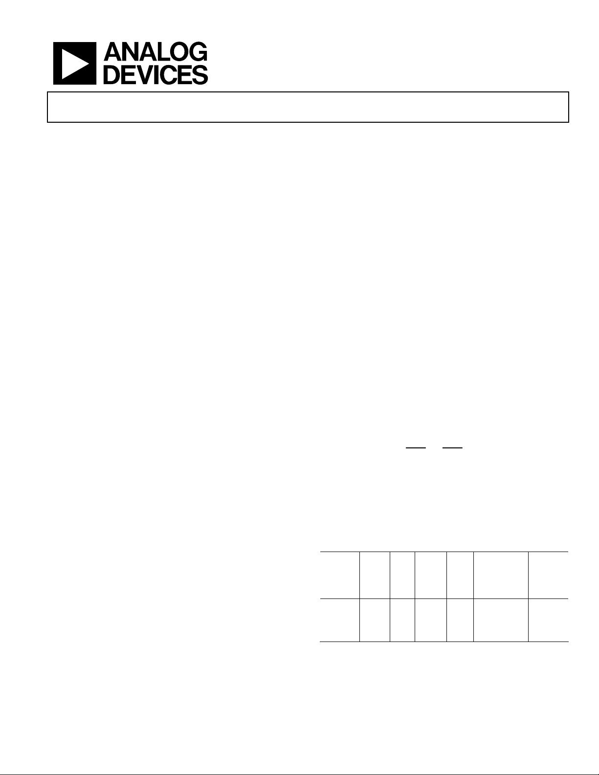
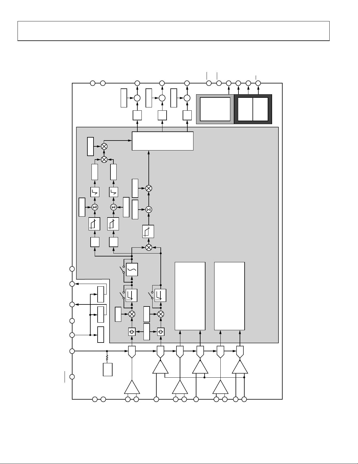
GENERAL DESCRIPTION
The ADE7854/ADE7858/ADE7868/ADE7878
1
are high
accuracy, 3-phase electrical energy measurement ICs with serial
interfaces and three flexible pulse outputs. The ADE78xx devices
incorporate second-order sigma-delta (Σ-Δ) analog-to-digital
converters (ADCs), a digital integrator, reference circuitry, and
all of the signal processing required to perform total (fundamental
1
U.S. patents pending.
and harmonic) active, reactive (ADE7878, ADE7868, and
ADE7858), and apparent energy measurement and rms calcu-
lations, as well as fundamental-only active and reactive energy
measurement (ADE7878) and rms calculations. A fixed function
digital signal processor (DSP) executes this signal processing.
The DSP program is stored in the internal ROM memory.
The ADE7854/ADE7858/ADE7868/ADE7878 are suitable for
measuring active, reactive, and apparent energy in various 3-phase
configurations, such as wye or delta services, with both three
and four wires. The ADE78xx devices provide system calibration
features for each phase, that is, rms offset correction, phase
calibration, and gain calibration. The CF1, CF2, and CF3 logic
outputs provide a wide choice of power information: total active,
reactive, and apparent powers, or the sum of the current rms
values, and fundamental active and reactive powers.
The ADE7854/ADE7858/ADE7868/ADE7878 contain wave-
form sample registers that allow access to all ADC outputs. The
devices also incorporate power quality measurements, such as
short duration low or high voltage detections, short duration
high current variations, line voltage period measurement, and
angles between phase voltages and currents. Two serial interfaces,
SPI and I
2
C, can be used to communicate with the ADE78xx. A
dedicated high speed interface, the high speed data capture
(HSDC) port, can be used in conjunction with I
2
C to provide
access to the ADC outputs and real-time power information.
The ADE7854/ADE7858/ADE7868/ADE7878 also have two
interrupt request pins,
IRQ0
and
IRQ1
, to indicate that an enabled
interrupt event has occurred. For the ADE7868/ADE7878, three
specially designed low power modes ensure the continuity of
energy accumulation when the ADE7868/ADE7878 is in a tam-
pering situation. See for a quick reference chart listing
each part and its functions. The ADE78xx are available in the
40-lead LFCSP, Pb-free package.
Table 1
Table 1. Part Comparison
Part No. WATT VAR
IRMS,
VRMS,
and
VA di/dt
Fundamental
WATT and
VAR
Tamper
Detect
and Low
Power
Modes
ADE7878 Yes Yes Yes Yes Yes Yes
ADE7868 Yes Yes Yes Yes No Yes
ADE7858 Yes Yes Yes Yes No No
ADE7854 Yes No Yes Yes No No
ADE7854/ADE7858/ADE7868/ADE7878
Rev. C | Page 2 of 92
TABLE OF CONTENTS
Features .............................................................................................. 1
Applications....................................................................................... 1
General Description......................................................................... 1
Revision History ............................................................................... 2
Functional Block Diagram .............................................................. 4
Specifications..................................................................................... 8
Timing Characteristics .............................................................. 11
Absolute Maximum Ratings.......................................................... 14
Thermal Resistance .................................................................... 14
ESD Caution................................................................................ 14
Pin Configuration and Function Descriptions........................... 15
Typical Performance Characteristics ........................................... 17
Test Circuit ...................................................................................... 19
Terminology .................................................................................... 20
Power Management........................................................................ 21
PSM0—Normal Power Mode (All Parts)................................ 21
PSM1—Reduced Power Mode (ADE7868, ADE7878 Only)21
PSM2—Low Power Mode (ADE7868, ADE7878 Only)....... 21
PSM3—Sleep Mode (All Parts) ................................................ 22
Power-Up Procedure.................................................................. 24
Hardware Reset........................................................................... 24
Software Reset Functionality .................................................... 25
Theory of Operation ...................................................................... 26
Analog Inputs.............................................................................. 26
Analog-to-Digital Conversion.................................................. 26
Current Channel ADC............................................................... 27
di/dt Current Sensor and Digital Integrator .............................. 29
Voltage Channel ADC ............................................................... 30
Changing Phase Voltage Datapath........................................... 31
Power Quality Measurements................................................... 32
Phase Compensation ................................................................. 37
Reference Circuit........................................................................ 39
Digital Signal Processor............................................................. 39
Root Mean Square Measurement............................................. 39
Active Power Calculation.......................................................... 43
Reactive Power Calculation—ADE7858, ADE7868, ADE7878
Only.............................................................................................. 48
Apparent Power Calculation..................................................... 53
Waveform Sampling Mode ....................................................... 56
Energy-to-Frequency Conversion............................................ 57
No Load Condition.................................................................... 60
Checksum Register..................................................................... 62
Interrupts..................................................................................... 63
Serial Interfaces .......................................................................... 64
ADE7878 Evaluation Board...................................................... 71
Die Version.................................................................................. 71
Silicon Anomaly ............................................................................. 72
ADE7854/ADE7858/ADE7868/ADE7878 Functionality
Issues ............................................................................................ 72
Functionality Issues.................................................................... 72
Section 1. ADE7854/ADE7858/ADE7868/ADE7878
Functionality Issues.................................................................... 73
Registers List ................................................................................... 74
Outline Dimensions ....................................................................... 92
Ordering Guide .......................................................................... 92
REVISION HISTORY
11/10—Rev. B to Rev. C
Change to Signal-to-Noise-and-Distortion Ratio, SINAD
Parameter, Table 1............................................................................. 9
Changes to Figure 18...................................................................... 18
Changes to Figure 22...................................................................... 19
Changes to Silicon Anomaly Section........................................... 72
Added Table 28 to Silicon Anomaly Section, Renumbered
Tables Sequentially ......................................................................... 73
8/10—Rev. A to Rev. B
Changes to Figure 1.......................................................................... 4
Changes to Figure 2.......................................................................... 5
Changes to Figure 3.......................................................................... 6
Changes to Figure 4.......................................................................... 7
Change to Table 8 ........................................................................... 16
Changes to Power-Up Procedure Section ................................... 23
Changes to Equation 6 and Equation 7 ....................................... 33
Changes to Equation 17................................................................. 43
Changes to Active Power Offset Calibration Section................ 45
Changes to Figure 63...................................................................... 46
Changes to Reactive Power Offset Calibration Section ............ 49
Changes to Figure 82...................................................................... 65
Added Silicon Anomaly Section, Renumbered Tables
Sequentially ..................................................................................... 71
ADE7854/ADE7858/ADE7868/ADE7878
Rev. C | Page 3 of 92
3/10—Rev. 0 to Rev. A
Added ADE7854, ADE7858, and ADE7878................... Universal
Reorganized Layout ...........................................................Universal
Added Table 1, Renumbered Sequentially.....................................1
Added Figure 1, Renumbered Sequentially ...................................3
Added Figure 2 ..................................................................................4
Added Figure 3 ..................................................................................5
Changes to Specifications Section...................................................7
Changes to Figure 9.........................................................................14
Changes to Table 8 ..........................................................................14
Changes to Typical Performance Characteristics Section .........16
Changes to Figure 22 ......................................................................18
Changes to the Power Management Section ...............................20
Changes to the Theory of Operation Section..............................25
Changes to Figure 31 and Figure 32 .............................................27
Change to Equation 28...................................................................47
Changes to Figure 83 ......................................................................66
Changes to Figure 86 ......................................................................68
Changes to the Registers List Section...........................................72
Changes to Ordering Guide...........................................................91
2/10—Revision 0: Initial Version
ADE7854/ADE7858/ADE7868/ADE7878
Rev. C | Page 4 of 92
FUNCTIONAL BLOCK DIAGRAM
PGA1
PGA1
PGA1
PGA3
PGA3
PGA3
1.2V
REF
DIGITAL SIGNAL
PROCESSOR
AVG AINAPHCAL
HPFDIS
[23:0]
HPF
AIGAIN
HPFDIS
[23:0]
DIGITAL
INTEGRATOR
HPF
POR LDO LDO
X
2
AIRMS
LPF
AIRMSOS
X
2
AVRMS
LPF
LPF
AVRMS OS
AVAGAIN
AWGAINAWATTOS
DFC
CFxDEN
:
DFC
CFxDEN
:
DFC
CFxDEN
:
52426 25174
7
8
9
22
12
13
14
19
18
39
37
38
36
32
29
35
34
33
3
2
27
28
23
6
SPI/I
2
C
I
2
C
RESET
REF
IN/OUT
VDD AGND AVDD DVDD DGND
CLKIN
CLKOUT
IAP
IAN
VAP
IBP
IBN
VBP
ICP
ICN
VCP
VN
PM0
PM1
CF1
CF2
CF3/HSCLK
IRQ0
IRQ1
SCLK/SCL
MOSI/SDA
MISO/HSD
SS/HSA
HSDC
ADE7854
ADC
ADC
ADC
ADC
ADC
ADC
08510-204
TOTAL ACTIVE/APPARENT
ENERGIES AND VOLTAGE/
CURRENT RMS CALCULATION FOR
PHASE C
(SEE PHASE A FOR DETAILED
DATA PATH)
TOTAL ACTIVE/APPARENT
ENERGIES AND VOLTAGE/
CURRENT RMS CALCULATION FOR
PHASE B
(SEE PHASE A FOR DETAILED
DATA PATH)
PHASE A,
PHASE B,
AND
PHASE C
DATA
Figure 1. ADE7854 Functional Block Diagram
ADE7854/ADE7858/ADE7868/ADE7878
Rev. C | Page 5 of 92
PGA1
PGA1
PGA1
PGA3
PGA3
PGA3
1.2V
REF
DIGITAL SIGNAL
PROCESSOR
COMPUTATIONAL
BLOCK FOR
TOTAL
REACTIVE POWER
AVGAINAPHCAL
HPFDIS
[23:0]
HPF
AIGAIN
HPFDIS
[23:0]
DIGITAL
INTEGRATOR
HPF
POR LDO LDO
X
2
AIRMS
LPF
AIRMSOS
X
2
AVRMS
LPF
LPF
AVRMSOS
AVAGAIN
AWGAINAWATTOS
AVARGAINAVAROS
DFC
CF1DEN
:
DFC
CF2DEN
:
DFC
CF3DEN
:
52426 25174
7
8
9
22
12
13
14
19
18
39
37
38
36
32
29
35
34
33
3
2
27
28
23
6
SPI/I
2
C
I
2
C
RESET
REF
IN/OUT
VDD AGND AVDD DVDD DGND
CLKIN
CLKOUT
IAP
IAN
VAP
IBP
IBN
VBP
ICP
ICN
VCP
VN
PM0
PM1
CF1
CF2
CF3/HSCLK
IRQ0
IRQ1
SCLK/SCL
MOSI/SDA
MISO/HSD
SS/HSA
HSDC
ADE7858
ADC
ADC
ADC
ADC
ADC
ADC
08510-203
TOTAL ACTIVE/REACTIVE/
APPARENT/ENERGIES AND
VOLTAGE/CURRENT
RMS CALCULATION FOR PHASE B
(SEE PHASE A FOR DETAILED
DATA PATH)
TOTAL ACTIVE/REACTIVE/
APPARENT/ENERGIES AND
VOLTAGE/CURRENT
RMS CALCULATION FOR PHASE C
(SEE PHASE A FOR DETAILED
DATA PATH)
PHASE A,
PHASE B,
AND
PHASE C
DATA
Figure 2. ADE7858 Functional Block Diagram
剩余91页未读,继续阅读
资源评论
wangxin19700
- 粉丝: 0
- 资源: 8
上传资源 快速赚钱
- 我的内容管理 展开
- 我的资源 快来上传第一个资源
- 我的收益 登录查看自己的收益
- 我的积分 登录查看自己的积分
- 我的C币 登录后查看C币余额
- 我的收藏
- 我的下载
- 下载帮助
安全验证
文档复制为VIP权益,开通VIP直接复制
信息提交成功