DS28E01中文资料

本文是英文数据资料的译文,文中可能存在翻译上的不准确或错误。如需进一步确认,请在您的设计中参考英文资料。
有关价格、供货及订购信息,请联络Maxim亚洲销售中心:10800 852 1249 (北中国区),10800 152 1249 (南中国区),
或访问Maxim的中文网站:china.maximintegrated.com。
AVAILABLE
``````````````````````````````````` গၤ
ET39F12.2112135ᆡFFQSPNᎧJTP0JFD!21229.4
ڔཝྲႯ)TIB.2*ࡼᒠኯሰ።ڔཝཱྀᑺஉᏴጙă
2135ᆡFFQSPNᑫᆐ႐Ljඛ367ᆡLjᄋ75ᆡ
ࡀ᎖ᒊቲቖݷᔫăჅᎌࡀ࣒ถᒙᆐቖۣઐ
ෝါLj݀భᒦጙᒙ᎖FQSPNᑞෝါLj૾ၫᆡ
ᒑถ࠭2ܤᆐ1ăඛຢET39F12.211ᎌᆎጙࡼ75ᆡSPN
ᓖݿ൩Ljᎅޣ૮రྜྷበຢăET39F12.211ᄰ߿࢛
2.Xjsf
®
ᔐሣᄰቧăᄰቧᔥክܪᓰࡼ2.XjsfፇLjᏴࣶৈ
ୈࡼ2.XjsfᆀᒦLjୈࡼᓖݿ൩భጲߠࡩஂ࢛ᒍă
``````````````````````````````````` ።
ࡌ፝૦ᒙᎧପހ
ጛࠅঢୂࢾᎧቅᓰ
ᇹᄻᒀဤޘཚۣઐ
``````````````````````````````````` ᄂቶ
♦ 2135ᆡFFQSPNࡀLjᆐ5Ljඛ367ᆡ
♦ ดᒙ623ᆡTIB.2༺Lj᎖ଐႯ271ᆡቧᇦཱྀᑺ൩
)NBD*݀ည߅මᏙ
♦ ቖᆰኊገᒀࡸමᏙ݀༦ถ৫ଐႯĂࠅ႙271ᆡNBDLj
ጲୂܰᑞᆗ
♦ ࡀᒦࡼ1Ă4ཝݝ႐భᎅઓᒙ
ᆐቖۣઐ
♦ 2భᎅઓܠ߈ᒙᆐPUQ!FQSPNᑞෝါ
)Đቖ1đ*ă
♦ Ꭷᓍ૦ମࡼᄰቧᄰവၫᔊቧږᑍ2.Xjsfፇ
ቲLjᄰቧႥൈᆐ26/4lcqt236lcqt
♦ ൝࢟ຳ༤ધ࢛ᒣૄ݆ᄋ೫ఝᐅဉถೆ
♦ ถ৫Ᏼ3/9Wᒗ6/36WኹᆍดቲࣗĂቖݷᔫLj
ᔫᏴ.51°Dᒗ,96°Dᆨࣞᆍ
♦ 7୭UTPDUEGOᓤ3୭TGOᓤ
ࡒTIB.2༺ۣઐࡼ
2Lᆡ2.Xjsf!FFQSPN
``````````````````````````````` ࢾ৪ቧᇦ
Rev 5; 7/10
ၫᓾ೯Ⴡቖ۾
+
ܭာᇄ)Qc*0SpITܪᓰࡼᓤă
UU'S!>!௳ࡒ۞ᓤă
*
FQ!>! ൡă
``````````````````````````` ࢜ቯᔫ࢟വ
2.XjsfဵNbyjn!Joufhsbufe!Qspevdut-!Jod/ࡼᓖݿܪă
୭ᒙᏴၫᓾ೯ࡼᔢઁ߲ă
༿ࣗᑗᓖፀǖ۾ᆪဵᅲᑳၫᓾ೯ࡼჁቖ۾Ljྙኊ༿ၫᓾ೯ཝᆪLj༿ᆰdijob/nbyjn.jd/dpn0ET39F12Lj࢛ૣ
༿ၫᓾ೯ཝᆪă
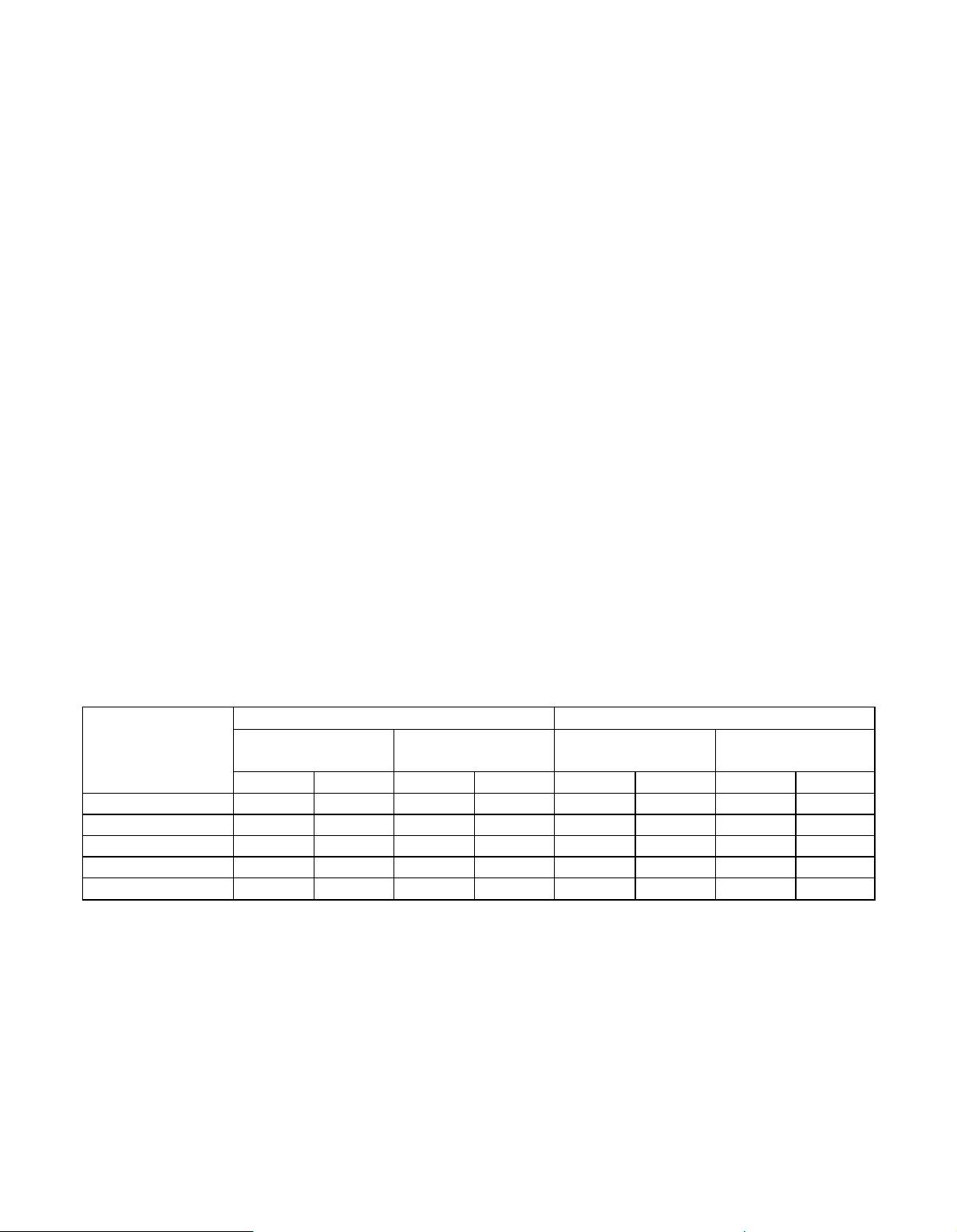
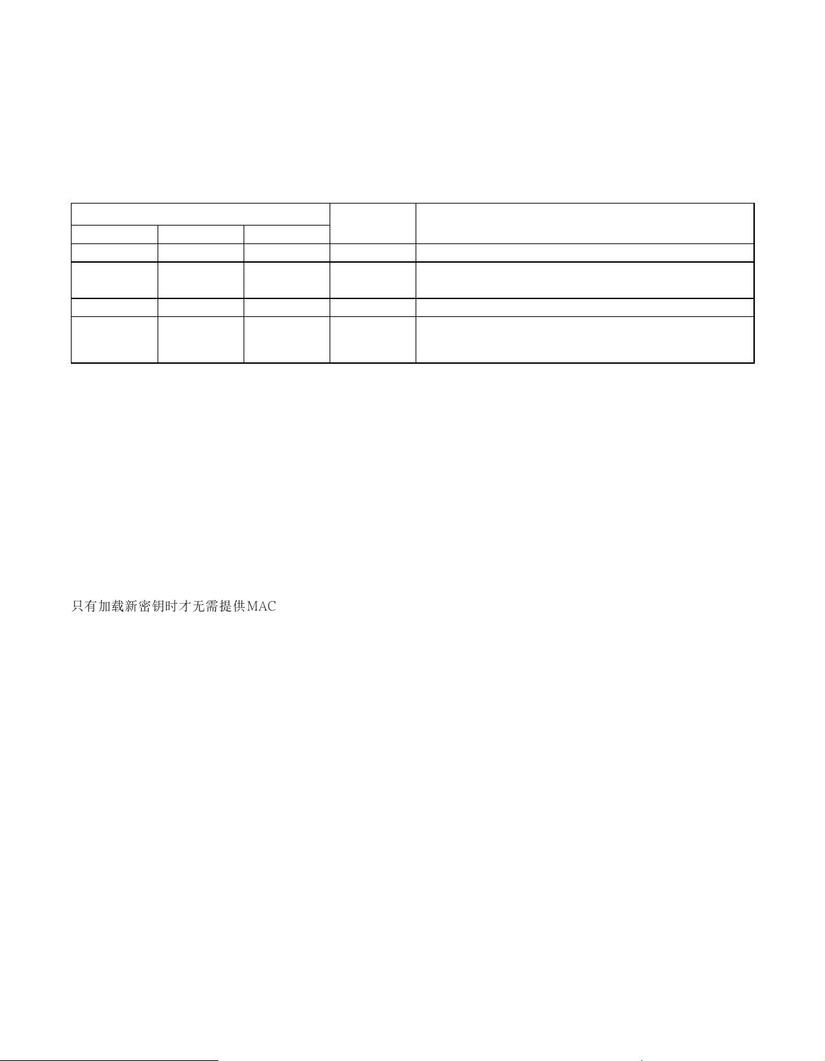
PART TEMP RANGE PIN-PACKAGE
DS28E01P-100+ -40°C to +85°C 6 TSOC
DS28E01P-100+T -40°C to +85°C 6 TSOC
DS28E01G-100+T&R -40°C to +85°C 2 SFN
DS28E01Q-100+T&R -40°C to +85°C
6 TDFN-EP*
(2.5k pcs)
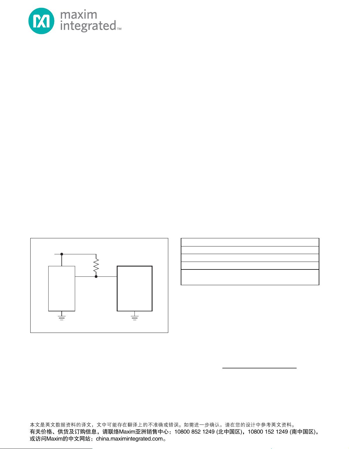
IO
R
PUP
V
CC
μC
GND
DS28E01-100
DS28E01-100
剩余20页未读,继续阅读
资源评论

 xtulcl2019-09-27还行,谢谢分享!
- qq_338849112019-09-03还不错,是中文的
 einsteinz2019-09-15不错,可以参考


