


Rev. 0.2 1/12 Copyright © 2012 by Silicon Laboratories AN627
AN627
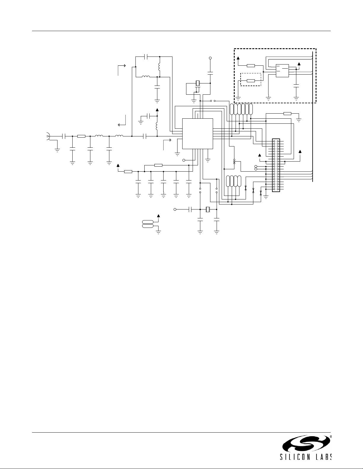
Si4460/61 LOW-POWER PA MATCHING
1. Introduction
This application note provides a description of the matching techniques applied to the low-power Si4460/61 RFIC
family. The typical power regime of the Si4461 is in the +13 to +16 dBm range, while the Si4460 is primarily
devoted to the +10 dBm applications.
Specifically, this document does not address the matching procedure for the PA on the Si4462/63/64 family of
RFICs. Because the output power level on the Si4463/64 family of RFICs is considerably higher than the Si4461/
60 RFIC, the matching procedure is somewhat different.
The matching network achieves a number of goals simultaneously:
Targets a nominal output power level of +10 to +16 dBm
Minimizes current consumption (i.e., maximize efficiency)
Constrains the peak voltage at the drain of the output devices
Complies with ETSI and FCC specifications for spurious emissions
Is immune against termination impedance variations as much as possible
Has low variation over temperature and supply voltage
Has low bill of materials and cost
Unfortunately, not all of these goals can be satisfied in the most optimal way simultaneously. Silicon Labs
investigates different matching types and methods to meet as much as possible with the above requirements. In
this document, the best two TX matching types (the switched PA mode Class E (CLE) type and the Switched
Current (SWC) type) are presented in detail.
Basically, the CLE type has the best efficiency. However, it has higher V
DD
and temperature variations; it’s current
consumption and the peak voltage on the TX pin are sensitive to the termination impedance variation, and it
usually requires slightly higher order filtering and thus higher bill of materials cost.
Another drawback of the Class E design is the inaccurate nonlinear power steps during power level adjustments.
The high V
DD
variation can be cured efficiently at low power levels (e.g., 10 dBm with 4460 or 14 dBm with 4461),
by the so-called adaptive power setting method. In this method the match is designed in such a way that the
specified power at the specified supply voltage is achieved at a relatively low power level setting. At decreasing
supply voltage (e.g., due to a discharging battery) the power drop can be compensated by the proper increase of
the power level setting i.e., with the decrease of the switcher loss. Unfortunately, this method works well only at
lower power regimes (+10 dBm with Si4460 and +14 dBm with Si4461) where a low power level setting is enough
to get the targeted power, and, thus, there is room for compensation. In these cases, the Class E stability over V
DD
can be even better than that of the switched current method.
A low power setting (at low power regimes) with higher switcher loss is also good to have immunity against
termination antenna impedance variations. It especially reduces the variation of the dc current consumption with
variable environmental conditions suffered by the antenna, which is favorable for long-life battery-operated
applications, such as meters or sensors, because the excess current drain is limited.
The SWC type matching usually has lower efficiency. But, with fixed power level setting it has better stability over
V
DD
and temperature (the CLE can be stable only with adaptive power setting). Another advantage of the SWC
solution is the accurate and linear power steps during power level tuning. Also it needs slightly weaker filtering and
thus slightly lower bill of materials. The design process is also simple compared to the CLE.
The matching procedure outlined in this document for CLE and SWC allows the user to achieve the above
mentioned properties and is applicable for two different types of board configurations: one with separate antennas
for the TX and RX paths (Split TX/RX board configuration) and one with a single antenna where the TX and RX
paths are tied directly together without the use of an RF switch (Direct Tie board configuration).


- 1
- 2
- 3
- 4
前往页