1880 IEEE JOURNAL OF SOLID-STATE CIRCUITS, VOL. 40, NO. 9, SEPTEMBER 2005
A 700
+
-mW Class D Design With Direct Battery
Hookup in a 90-nm Process
Brett Forejt, Senior Member, IEEE, Vijay Rentala, Jose Duilio Arteaga, and Gangadhar Burra
Abstract—A “battery connect” compatible class D (switching)
amplifier which is fully integrated in a 90-nm digital CMOS
process is presented. The integration of the amplifier requires no
additional masks, processing, or cost. This paper includes a brief
description of the circuit techniques that enable direct battery
(2.7–5.4 V) connection and allow support
6 7V
P2P
(700 mW
into 8
) output swing from a 4.2-V supply using devices that
operate solely with low gate voltages. The achieved SNR over
an audio (20 Hz to 20 kHz) bandwidth
98 5
dB and the total
harmonic distortion (THD) is better than 0.03% at 500 mW.
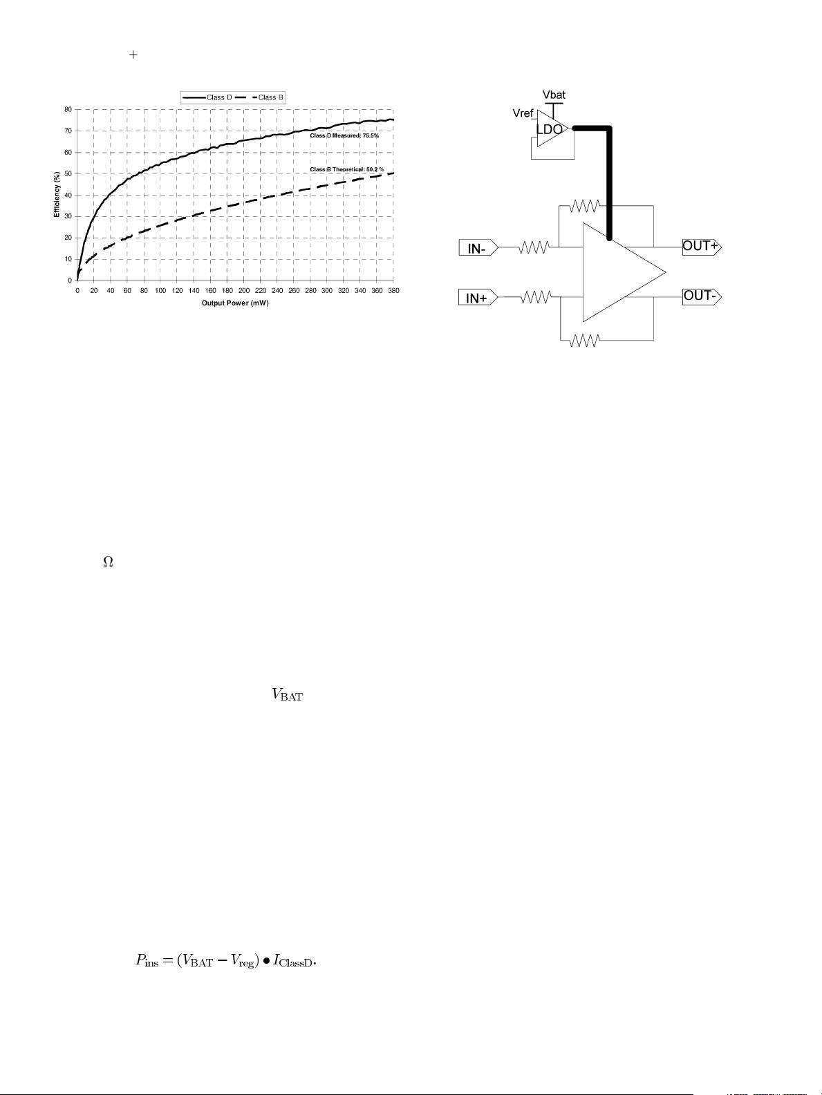
Efficiency is greater than 75% above 375 mW. The power supply
rejection ratio, which is a crucial parameter in modules connected
directly to the battery, is measured at 70 dB at 217 Hz. The area of
the switching amplifier is
0 44
mm
2
, where the power devices
occupy approximately 20% of the total.
Index Terms—Class D amplifier, common mode rejection ratio
(CMRR), efficiency, electromagnetic interference (EMI), low
drop-out regulator (LDO), power supply rejection ratio (PSRR),
pulse-width modulation (PWM), signal-to-noise ratio (SNR),
system-on-chip (SOC), total harmonic distortion (THD), ultra-
deep submicron (UDSM).
I. INTRODUCTION
C
LASS D amplifiers, due to their high efficiencies, are ex-
tremely attractive for systems-on-chip (SOCs) for mobile
and low-power applications, where battery life and reduced heat
are crucial parameters. Obtaining these efficiencies mandates
that the switching amplifiers are directly connected to the bat-
tery instead of a linear or a switching regulator output. Typical
handset battery voltages range from 2.7 to 5.4 V.
Continuous-time output amplifiers have a theoretical effi-
ciency of 78.5% and applied efficiencies near 30% while Class
D can approach 100% in theory and has practical efficiencies
of 70% or greater. More efficient power usage reduces wasted
battery energy which in turn increases battery life and reduces
the amount of heat generated by the device. Battery life and
reduced heat are important factors in the feasibility of SOC
designs.
Typical battery voltages in mobile technologies range from
as low as 2.7 V to as high as 4.8 V. During charging conditions,
the battery terminals may be as high as 5.4 V DC. These voltage
levels present a problem in ultradeep submicron (UDSM) pro-
cesses due to the fact that the maximum voltage rating of the
gate oxide is typically less than 1.5 V. In order to produce a
transistor that is reliable under these gate voltage stresses, extra
Manuscript received December 13, 2004; revised March 8, 2005. This work
was supported by Texas Instruments Incorporated.
The authors are with Texas Instruments, Inc., Dallas, TX 75243 USA (e-mail:
bforejt@ti.com; rvijay@ti.com; jarteaga@ti.com; gburra@ti.com).
Digital Object Identifier 10.1109/JSSC.2005.848147
processing is normally required for each wafer. This extra pro-
cessing decreases the profitability of the design.
Using a standard 90-nm digital process with no mask or pro-
cessing adders, we have achieved
700-mW output Class D am-
plifier with direct battery hookup. The SNR is
98.5 dB and the
THD is better than 0.03% at full power. The PSRR of the system
is measured at
70 dB at 217 Hz. The area is mm .
II. P
RIOR
ART
There are two main approaches to the design of class D am-
plifiers: open loop and closed loop. The open-loop approach
directly feeds signal into the PWM generator. The output of
the PWM generator drives the output stage [8]. The open-loop
approach offers reasonable performance but suffers from poor
supply and substrate noise rejection. Due to the noise present
on the battery because of various other blocks in an SOC, the
power supply rejection and substrate noise rejection degrade the
quality of the audio signal at the output.
The closed-loop systems use negative feedback to improve
the performance of the Class D amplifier. Feedback systems in-
herently offer higher supply and substrate noise rejection. The
amount of rejection can be improved by increasing the order of
the loop filter [7].
Class D amplifiers with binary PWM modulation require ex-
ternal filters to reconstruct the signal and reduce electromag-
netic interference (EMI). There are techniques that may relax
the output filter requirement by using digital signal processing
techniques [1]. Double-sided natural sampling PWM modula-
tion or ternary PWM modulation relaxes the requirements for
the external filtering [5].
The other major issue in the design of class D in a deep sub-
micron process is the device limitations. There are few known
techniques to overcome these device limitations like the use of
level shifters [8].
Presented herein is a simple first-order closed-loop architec-
ture with ternary modulation that does not require any external
filter and directly hooks up to a battery in a process that does not
allow voltages more than 1.5 V across gate and source terminals.
III. D
ESIGN CHALLENGES
Low-efficiency designs dissipate power locally on chip, thus
generating an unacceptable amount of heat. For Example, if 1 W
is delivered to the load from a 50% efficient design, 1 W must
be dissipated inside the package for just this one function! The
adverse affects of heat in integrated circuits are well known [9],
and at its limit the temperature increase can cause damage to the
device [10].
0018-9200/$20.00 © 2005 IEEE


 我的内容管理
展开
 我的资源
快来上传第一个资源
 我的收益 登录查看自己的收益
 我的积分
登录查看自己的积分
 我的C币
登录后查看C币余额
 我的收藏
我的收藏  我的下载
我的下载  下载帮助
下载帮助 
 前往需求广场,查看用户热搜

 信息提交成功