音频功放芯片AW87359 datasheet
需积分: 3 99 浏览量
2024-04-30
15:49:47
上传
评论
收藏 3.42MB PDF 举报

AW87359
Dec. 2019 V1.1
www.awinic.com.cn COPYRIGHT ©2019 SHANGHAI AWINIC TECHNOLOGY CO., LTD.
1
High Efficiency Low Noise Large Volume Handsets Stereo
TLTR-AGC 3
rd
Smart K Audio Amplifier
FEATURES
Triple-Level Triple-Rate AGC algorithm:
Enhance bass, improve the dynamic range
Increase volume, eliminate noise, timely and
effectively protect the speaker
Output Power:3.1W@8Ω,3.5W@6Ω
Low Noise:11μV
Low THD+N:0.02%
Overall efficiency up to 80%
Support high power receiver stereo application
Support AB/D speaker , AB/D receiver 2-in-1
application
AB receiver:0dB,Vn=11μV,THD+N=0.2%
D receiver:4.5dB,Vn=16μV,THD+N=0.02%
Support 1.8V I2C Control
Over current protection, over-temperature
protection and short-circuit protection
Super TDD-Noise suppression
Excellent pop-click suppression
High PSRR:-90dB(217Hz)
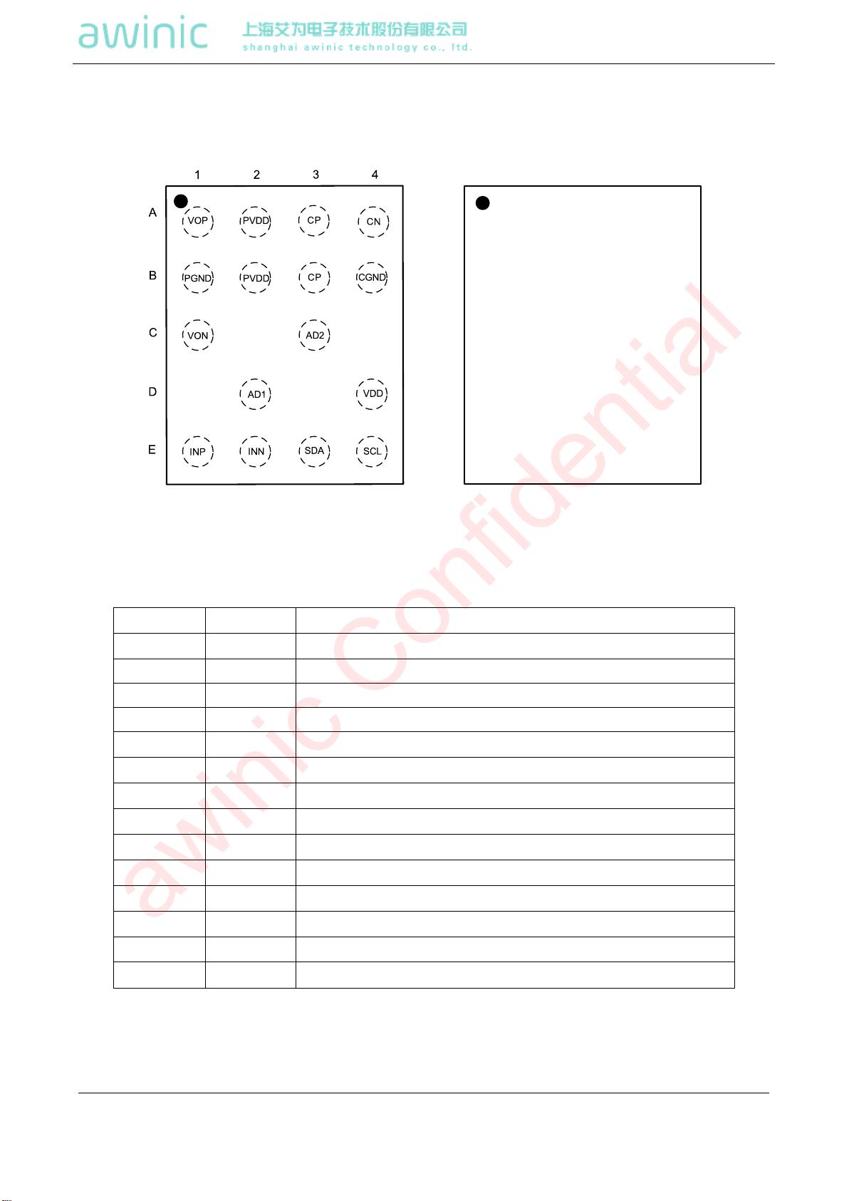
FCQFN 2.5mmX2.0mmX0.55mm-16L package
APPLICATIONS
Smart phone、Tablet PC、Tactile feedback
DESCRIPTION
AW87359 is specifically designed to improve the
musical output dynamic range, enhance the overall sound
quality, which is a new high efficiency, low noise, constant
large volume, 3rd Smart K audio amplifier. AW87359
integrates awinic’s proprietary Triple-Level Triple-Rate AGC
audio algorithm, effectively eliminating music noise and
improving sound quality and volume. AW87359 integrated
efficiency up to 90% of high voltage DO-Chargepump
technology, significantly improving the dynamic range of the
music output. AW87359 noise floor is as low as to 38μV at
speaker mode, with 102dB high signal-to-noise-ratio (SNR).
The ultra-low distortion 0.02% and unique Triple-Level
Triple-Rate AGC technology bring high quality music
enjoyment.
AW87359 support speaker and high power receiver
stereo applications;supports speaker and receiver 2-in-1
applications,class AB/D receiver optional,ultra-low noise is
11μV.
AW87359 controls internal registers through the I
2
C
interface. Register parameters include output voltage, power
amplifier gain, Triple-Level Triple-Rate AGC parameters etc.
AW87359 built-in over current protection, over
temperature protection and short circuit protection function,
effectively protect the chip. AW87359 features small FCQFN
2.5mmX2.0mmX0.55mm-16L package.
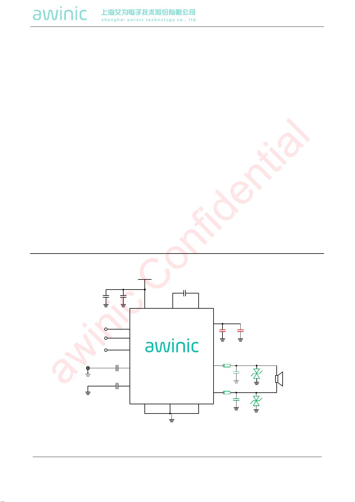
TYPICAL APPLICATION CIRCUIT
VBAT
AW87359
VDD
PVDD
VOP
VON
INN
INP
CN
SDA
SCL
AD1
I
2
C Interface
I
2
C Address Select
SPK
AD2 CGND PGND
C3 B4 B1
{
E3
E4
D2
E1
E2
D4
C5
100nF
C6
100nF
C2
0.1uF
C3
10uF
A3,B3
A2,B2
C0
10uF
25V
C1
10uF
25V
B1
C7
0.1nF
16V
B2
C8
0.1nF
16V
A1
C1
12V
12V
CP
A4
C4
4.7uF
Figure 1 AW87359 Single-ended input mode Application Diagram
awinic Confidential


剩余44页未读,继续阅读
资源评论


