Power Driver Integrated Full Digital Audio Amplifier NTP8835C
Copyright ⓒ NeoFidelity, Inc. Page 3
Document Number: NTP8835C Rev1.0 2021-04-27
Table of Contents
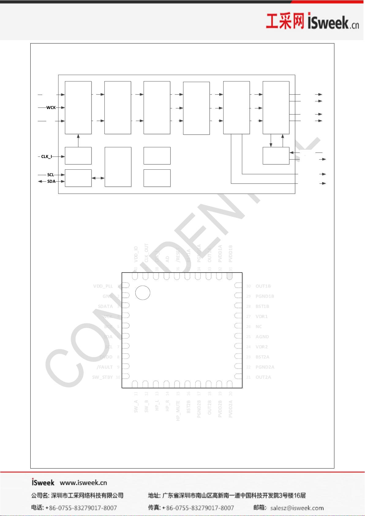
1. BLOCK DIAGRAM ....................................................................................................................................................... 4
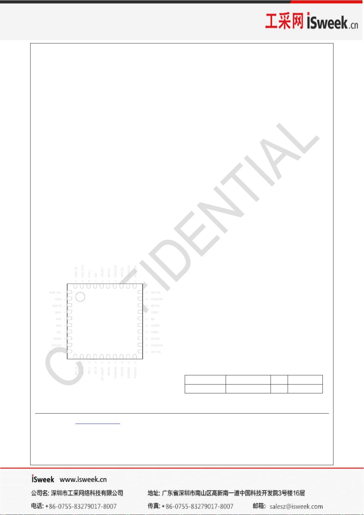
2. PIN ASSIGNMENTS ..................................................................................................................................................... 4
3. PIN DESCRIPTIONS .................................................................................................................................................... 5
4. CHARACTERISTICS AND SPECIFICATIONS ............................................................................................................ 6
4.1. Absolute Maximum Ratings .................................................................................................................................... 6
4.2. Recommended Operating Conditions .................................................................................................................... 6
4.3. DC Electrical Characteristics .................................................................................................................................. 6
4.4. PLL Input Parameters and External Filter Components ......................................................................................... 7
4.5. Performance Specification ...................................................................................................................................... 7
4.6.1 Switching Characteristics – I
2
C Control ................................................................................................................ 8
4.6.2 Switching Characteristics – Audio Interface .......................................................................................................... 8
5. I
2
C BUS OF NTP8835C ................................................................................................................................................ 9
5.1. General Description of I
2
C Bus ............................................................................................................................... 9
5.1.1. Writing Operation................................................................................................................................................. 9
5.1.2. Reading Operation ............................................................................................................................................ 11
5.2 I
2
C Glitch Filter ...................................................................................................................................................... 12
6. CLOCK, RESET & CONTROL ................................................................................................................................... 13
6.1. System Clock ....................................................................................................................................................... 13
6.2. Timing Sequence (recommend) ........................................................................................................................... 13
6.2.1. Power-Up & Initialization Sequence .................................................................................................................. 13
6.2.2. Power-Down Sequence ..................................................................................................................................... 13
6.3. Timing Sequence 2 (reference) ............................................................................................................................ 14
6.3.1. Power-Up & Initialization Sequence .................................................................................................................. 14
6.3.2. Power-Down Sequence ..................................................................................................................................... 14
6.4. Sound On/Off Sequence ...................................................................................................................................... 15
6.4.1. 2-channel Sound On/Off Sequence ................................................................................................................... 15
6.4.2. 2.1-channel Sound On/Off Sequence ................................................................................................................ 15
7. AUDIO INPUT ............................................................................................................................................................ 16
7.1. I
2
S and Serial Audio Interface ............................................................................................................................... 16
7.1.1. I
2
S Glitch Filter................................................................................................................................................... 16
7.2. SDATA Generator ................................................................................................................................................. 16
7.3. Asynchronous Sample Rate Conversion .............................................................................................................. 16
8. MIXER ........................................................................................................................................................................ 18
9. PRE-PROCESSING ................................................................................................................................................... 19
9.1. Pre Bi-Quad Filter Chain ...................................................................................................................................... 19
9.2. 3D Surround ......................................................................................................................................................... 19
9.3. Configurable Graphic Equalizer ............................................................................................................................ 20
9.4. Post Bi-Quad Filter Chain ..................................................................................................................................... 20
9.5. Loudness Control ................................................................................................................................................. 21
10. VOLUME & DYNAMIC RANGE CONTROL ............................................................................................................... 22
10.1. Master Volume Control ....................................................................................................................................... 22
10.2. Channel Volume Control..................................................................................................................................... 22
10.3. Master Volume Fine Control ............................................................................................................................... 22
10.4. Mute and Soft Volume Change ........................................................................................................................... 22
10.5. Auto Mute ........................................................................................................................................................... 22
10.6. Dynamic Range Control ..................................................................................................................................... 23
11. OUTPUT INTERFACE ................................................................................................................................................ 24
11.1. Output Configuration ........................................................................................................................................... 24
11.2. AM Interference Relief Mode .............................................................................................................................. 24
11.3. PWM Output Mapper .......................................................................................................................................... 24
11.4. Switching Output Mode ....................................................................................................................................... 24
11.5. Soft Start ............................................................................................................................................................. 25
12. TYPICAL APPLICATION SCHEMATICS (2 Channel) ............................................................................................... 26
13. TYPICAL APPLICATION SCHEMATICS (2.1 Channel) ............................................................................................ 27
14. TYPICAL APPLICATION SCHEMATICS (PBTL) ....................................................................................................... 28
15. APPENDIX ................................................................................................................................................................. 29
A. Configuration Register Summary ........................................................................................................................ 29
B. Configuration Register Value Reference ............................................................................................................. 46
C. Typical Characteristics Graph .............................................................................................................................. 51
D. Outline and Mechanical Data .............................................................................................................................. 67