
Analog Circuit and Device Interaction in High-Speed SerDes Design in 16nm
FinFET CMOS Technology
Freeman Zhong, Ashutosh Sinha
Avago Technologies Inc, San Jose, CA 95131
Abstract
SerDes deals with data serialization, deserialization and
channel equalization up to data rate of 28+Gb/s. Process
technology and device characteristic greatly impacts
architecture, circuit topology, and design merit of a SerDes.
Several architecture choices, analog circuits, and techniques
to mitigate undesired device characteristic in 16nm FinFET
are discussed in this paper. With advanced CMOS technology
and mitigation techniques, a prototype 28Gb/s SerDes was
developed and demonstrated desired performance, power and
die area.
Introduction
SerDes is one of the most critical components in
communication systems. As data traffic increases
exponentially and CMOS technology advances to 16nm in
past 15 years, data rate of SerDes has increased from
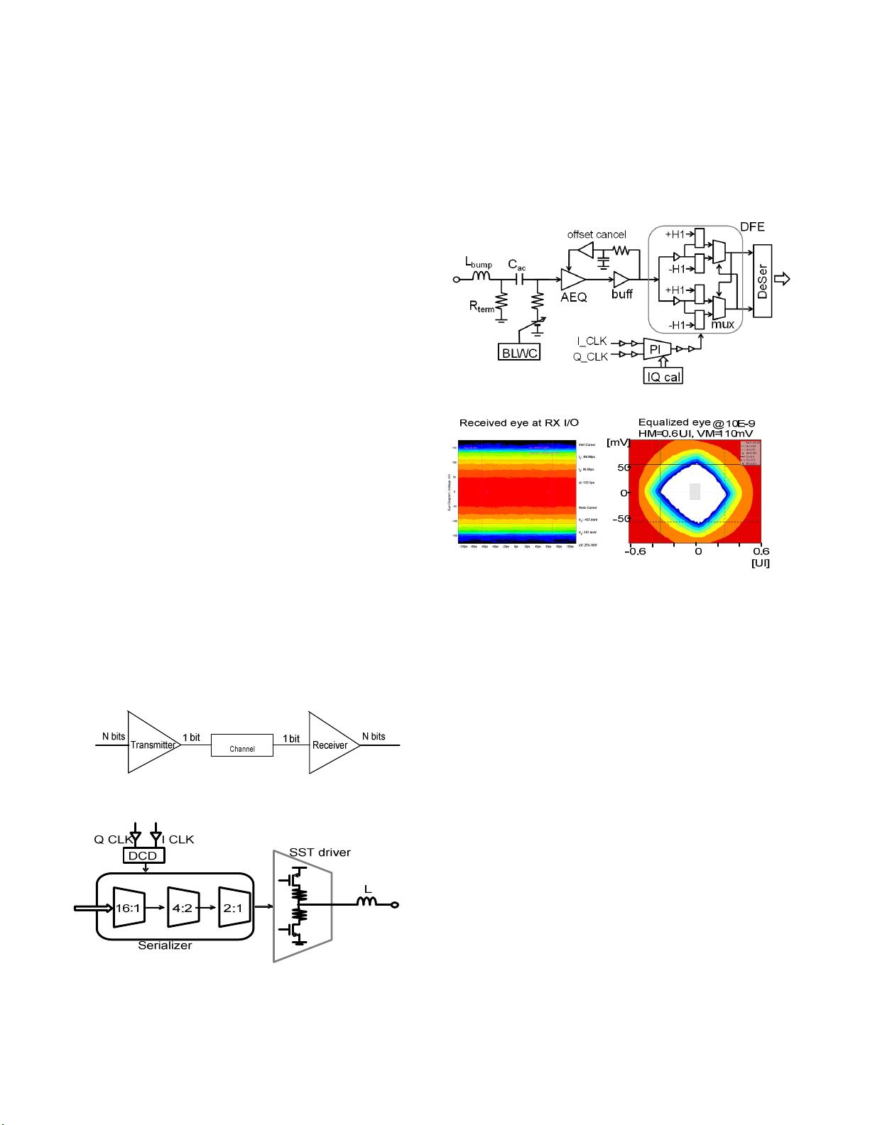
1.25Gb/s to 28+Gb/s. As shown in Fig. 1, 2, 3, a serial link
consists of a transmitter, channel, and receiver. It not only
functions as data serialization from N to 1 bit, and
deserialization from 1 to N bit, but also deals with signal
integrity challenges, such as inter-symbol-interference, cross-
talk, reflection and system jitter as data rate increases. Due to
low-pass nature of a channel, the received eye is totally
closed at a receiver. With channel equalization from both
transmitter and receiver, the equalized eye is open enough for
clock and data recovery as shown in Fig. 4. Many SerDes
were designed and fabricated in 250nm to 28nm CMOS
technology (1), (2), (3).
Fig. 1– Block diagram of a serial link
Fig. 2 – Block diagram of a transmitter
Figure 3 – Block diagram of a receiver
Fig. 4 – Received and equalized eyes at a receiver with 28Gb/s PRBS31 data
traffic over a channel of 34dB loss
SerDes architecture and process technology interaction
Process technology greatly impacts the architecture,
implementation, performance and power consumption of a
SerDes. The critical process parameters, such as unity gain
frequency, threshold voltage, leakage, and maximum supply
voltage of devices, are dominant considerations for SerDes
architecture choice. For example, a decision feedback
equalizer (DFE) is a timing critical circuit that generates a
feedback signal and adds it to the received signal within one
unit interval (UI). For data rate below 16Gb/s, direct
feedback DFE, as shown in Fig. 5, is an optimal
implementation where the timing constraint of Tck-q + Tdac
+ Tsum + Tsetup < 1UI can be met in in 28nm/16nm process.
However, when data rate increases to 28Gb/s where 1UI is
only 35.7ps, the timing constraint of direct DFE is no longer
met. A h1 loop unrolled DFE, shown in Fig. 6, was
developed where the +/-h1 feedback signals are pre-
calculated and added to received signal, and 2 speculative
outputs are selected based on previous data decision, thus,
new timing constraint of Tck-q + Tmux + Tsetup < 1UI can
be met in 28nm/16nm CMOS.
As CMOS technology scales down to16nm, thin-oxide device
operates at lower supply voltage that presents challenges of
headroom and linearity to analog circuits. To tackle these
3.2.1 IEDM14-52978-1-4799-8001-7/14/$31.00 ©2014 IEEE
资源评论

 ddalecn2019-03-20文档不错,好好学习。

whyyfdr
- 粉丝: 7
- 资源: 9


最新资源
- Comsol锂枝晶模型构建指南:相场法实现单枝晶与多枝晶定向生长,三场耦合新手入门教程,基于相场法的COMSOL锂枝晶模型构建:从单枝晶到多枝晶的定向生长及三种物理场耦合实战指南,Comsol锂枝晶
- 基于多松弛(MRT)模型的格子玻尔兹曼方法(LBM)Matlab代码实现:模拟压力驱动流场与优化算法研究,使用多松弛(MRT)模型与格子玻尔兹曼方法(LBM)模拟压力驱动流的Matlab代码实现,使用
- 永磁同步电机自抗扰控制模型:ADRC技术及其应用研究,永磁同步电机自抗扰控制模型ADRC:原理、应用与优化探讨,永磁同步电机自抗扰控制模型ADRC ,永磁同步电机; 自抗扰控制模型; ADRC,永磁同
- **全自动驾驶框架下的汽车纵向与横向协同控制技术研究**,自动驾驶中的纵向与横向控制技术研究与应用-全自动驾驶系统优化策略与路径跟踪性能评估,#汽车纵向和横向控制 本项目涉及在全自动驾驶框架内进行汽
- 工具变量-引导基金数据集.xlsx
- 2010年下半年软件设计师考试上午真题-真题及答案解析
- 激光熔覆仿真技术研究:温度与应力分布的耦合仿真与动画呈现,激光熔覆仿真技术研究:温度与应力分布的耦合仿真及动画展示,【激光熔覆仿真】 1、通过激光进行熔覆工艺进行仿真,对温度与应力进行研究 2、采用C
- COMSOL模拟:离子迁移与PH变化动态分析在电场、流场及稀物质传递物理场的应用研究,COMSOL模拟离子迁移与PH变化:电场、流场及稀物质传递三物理场的综合应用,comsol模拟离子迁移PH变化
- 基于Simulink的磁流变半主动悬架模型构建及策略设计,磁流变半主动悬架Simulink模型的创建与策略设计攻略,磁流变半主动悬架simulink模型,包含模型创建,模型策略设计 ,磁流变半主动悬架
- 基于二维comsol的Voronoi分析:灵活设置边界与过渡界面厚度,适用于ABAQUS与AUTOCAD辅助生成的多边形与纤维骨料建模,二维Comsol Voronoi技术:支持多种边界设置与ABAQ
- VIENNA维也纳拓扑三相整流Simulink仿真:电压电流双闭环控制策略,电压外环PI控制,电流内环Bang-Bang滞环控制实现稳压输出至600V-参考资料附后,VIENNA维也纳拓扑三相整流S
- 基于三有源桥的模型预测控制仿真:独立控制输出侧端口电压与电流,快速动态响应及四有源桥电路扩展应用,基于三有源桥的模型预测控制仿真:独立控制输出侧电压电流,快速动态响应,可拓展至四有源桥电路研究,基于三
- ANSYS Fluent电机流体场与温度场分析实战教程:多方式冷却电机仿真分析全流程与技巧,ANSYS Fluent电机流体场与温度场深度解析教程:多种冷却方式下的电机仿真分析流程与方法,ansys
- LockSupport
- HCIA数通(RS)培训视频.zip
- 电脑端查看apk各种信息的工具
资源上传下载、课程学习等过程中有任何疑问或建议,欢迎提出宝贵意见哦~我们会及时处理!
点击此处反馈


