没有合适的资源?快使用搜索试试~ 我知道了~
ADE7753 的片内数字积分器能以优良精度的数字积分作用 , 实现在频域内,将- 20dB/10 倍频程衰减和一种固定的 -90( 相移作用。数字积分器的相频响应和幅频响 应非常接近于理想情况。片内数字积分器提供直接接口到 di/dt 微分电流传感器, 从而省去了外部的模拟积分器,因而保证极好的长时间稳定性,与高精度的电压
资源推荐
资源详情
资源评论
Single-Phase Multifunction Metering IC
with di/dt Sensor Interface
ADE7753
Rev. B
Information furnished by Analog Devices is believed to be accurate and reliable.
However, no responsibility is assumed by Analog Devices for its use, nor for any
infringements of patents or other rights of third parties that may result from its use.
Specifications subject to change without notice. No license is granted by implication
or otherwise under any patent or patent rights of Analog Devices. Trademarks and
registered trademarks are the property of their respective owners.
One Technology Way, P.O. Box 9106, Norwood, MA 02062-9106, U.S.A.
Tel: 781.329.4700 www.analog.com
Fax: 781.326.8703 ©2003–2009 Analog Devices, Inc. All rights reserved.
FEATURES
High accuracy; supports IEC 60687/61036/61268 and
IEC 62053-21/62053-22/62053-23
On-chip digital integrator enables direct interface to current
sensors with di/dt output
A PGA in the current channel allows direct interface to
shunts and current transformers
Active, reactive, and apparent energy; sampled waveform;
current and voltage rms
Less than 0.1% error in active energy measurement over a
dynamic range of 1000 to 1 at 25°C
Positive-only energy accumulation mode available
On-chip user programmable threshold for line voltage surge
and SAG and PSU supervisory
Digital calibration for power, phase, and input offset
On-chip temperature sensor (±3°C typical)
SPI® compatible serial interface
Pulse output with programmable frequency
Interrupt request pin (
IRQ
) and status register
Reference 2.4 V with external overdrive capability
Single 5 V supply, low power (25 mW typical)
GENERAL DESCRIPTION
The ADE7753
1
features proprietary ADCs and DSP for high
accuracy over large variations in environmental conditions and
time. The ADE7753 incorporates two second-order 16-bit Σ-Δ
ADCs, a digital integrator (on CH1), reference circuitry,
temperature sensor, and all the signal processing required to
perform active, reactive, and apparent energy measurements,
line-voltage period measurement, and rms calculation on the
voltage and current. The selectable on-chip digital integrator
provides direct interface to di/dt current sensors such as
Rogowski coils, eliminating the need for an external analog
integrator and resulting in excellent long-term stability and pre-
cise phase matching between the current and voltage channels.
The ADE7753 provides a serial interface to read data, and a
pulse output frequency (CF), which is proportional to the active
power. Various system calibration features, i.e., channel offset
correction, phase calibration, and power calibration, ensure
high accuracy. The part also detects short duration low or high
voltage variations.
The positive-only accumulation mode gives the option to
accumulate energy only when positive power is detected. An
internal no-load threshold ensures that the part does not exhibit
any creep when there is no load. The zero-crossing output (ZX)
produces a pulse that is synchronized to the zero-crossing point
of the line voltage. This signal is used internally in the line cycle
active and apparent energy accumulation modes, which enables
faster calibration.
The interrupt status register indicates the nature of the interrupt,
and the interrupt enable register controls which event produces
an output on the
IRQ
pin, an open-drain, active low logic output.
The ADE7753 is available in a 20-lead SSOP package.
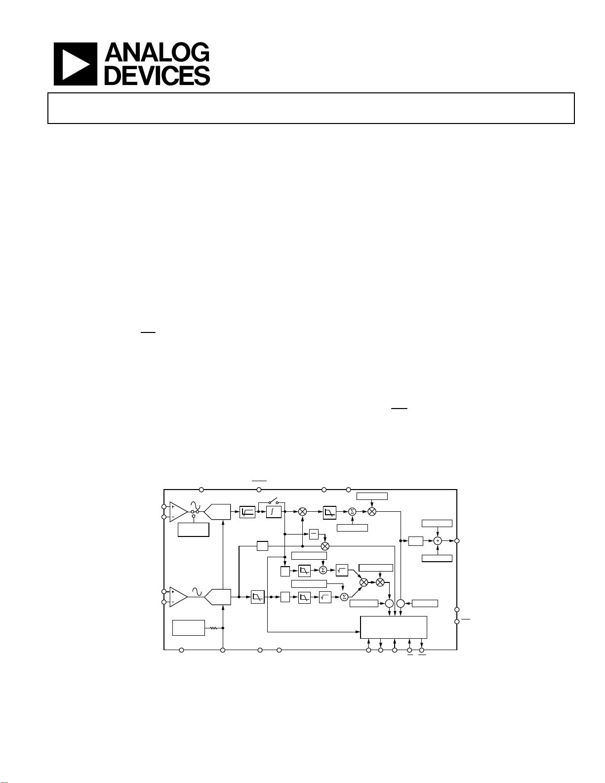
FUNCTIONAL BLOCK DIAGRAM
AVDD
RESET
DVDD DGND
TEMP
SENSOR
ADC
ADC
DFC
x
2
ADE7753
LPF2
MULTIPLIER
INTEGRATOR
CLKIN
CLKOUT
DIN DOUT SCLKREF
IN/OUT
CS IRQ
AGND
APOS[15:0]
VAGAIN[11:0]
VADIV[7:0]
IRMSOS[11:0]
VRMSOS[11:0]
WGAIN[11:0]
dt
REGISTERS AND
SERIAL INTERFACE
CFNUM[11:0]
CFDEN[11:0]
2.4V
REFERENCE
4k
PHCAL[5:0]
HPF1
LPF1
02875-A-001
V1P
V1N
V
2N
V2P
PGA
PGA
ZX
SAG
CF
WDIV[7:0]
% %
Φ
π
2
x
2
Figure 1.
1
U.S. Patents 5,745,323; 5,760,617; 5,862,069; 5,872,469; others pending.
ADE7753
Rev. B | Page 2 of 60
TABLE OF CONTENTS
Specifications ..................................................................................... 4
Timing Characteristics ..................................................................... 6
Absolute Maximum Ratings ............................................................ 7
ESD Caution .................................................................................. 7
Terminology ...................................................................................... 8
Pin Configuration and Function Descriptions ............................. 9
Typical Performance Characteristics ........................................... 11
Theory of Operation ...................................................................... 16
Analog Inputs .............................................................................. 16
di/dt Current Sensor and Digital Integrator ........................... 17
Zero-Crossing Detection ........................................................... 18
Period Measurement .................................................................. 19
Power Supply Monitor ............................................................... 19
Line Voltage Sag Detection ....................................................... 19
Peak Detection ............................................................................ 20
ADE7753 Interrupts ................................................................... 21
Temperature Measurement ....................................................... 22
ADE7753 Analog-to-Digital Conversion ................................ 22
Channel 1 ADC .......................................................................... 23
Channel 2 ADC .......................................................................... 25
Phase Compensation .................................................................. 27
Active Power Calculation .......................................................... 28
Energy Calculation ..................................................................... 29
Power Offset Calibration ........................................................... 31
Energy-to-Frequency Conversion ............................................ 31
Line Cycle Energy Accumulation Mode ................................. 33
Positive-Only Accumulation Mode ......................................... 33
No-Load Threshold .................................................................... 33
Reactive Power Calculation ...................................................... 34
Sign of Reactive Power Calculation ......................................... 35
Apparent Power Calculation ..................................................... 35
Apparent Energy Calculation ................................................... 36
Line Apparent Energy Accumulation ...................................... 37
Energies Scaling .......................................................................... 38
Calibrating an Energy Meter Based on the ADE7753 ........... 38
CLKIN Frequency ...................................................................... 48
Suspending ADE7753 Functionality ....................................... 48
Checksum Register..................................................................... 48
ADE7753 Serial Interface .......................................................... 49
ADE7753 Registers ......................................................................... 52
ADE7753 Register Descriptions ................................................... 55
Communications Register ......................................................... 55
Mode Register (0x09) ................................................................. 55
Interrupt Status Register (0x0B), Reset Interrupt Status
Register (0x0C), Interrupt Enable Register (0x0A) ............... 57
CH1OS Register (0x0D) ............................................................ 58
Outline Dimensions ....................................................................... 59
Ordering Guide .......................................................................... 59
ADE7753
Rev. B | Page 3 of 60
REVISION HISTORY
1/09—Rev. A to Rev B
Changes to Features Section ............................................................ 1
Changes to Zero-Crossing Detection Section and Period
Measurement Section ..................................................................... 19
Changes to Channel 1 RMS Calculation Section, Channel 1
RMS Offset Compensation Section, and Equation 4 ................. 25
Changes to Figure 56 and Channel 2 RMS Calculation
Section .............................................................................................. 26
Changes to Figure 57 ...................................................................... 27
Changes to Energy Calculation Section ....................................... 30
Changes to Energy-to-Frequency Conversion Section .............. 31
Changes to Apparent Energy Calculation Section...................... 36
Changes to Line Apparent Energy Accumulation Section ........ 37
Changes to Table 10 ........................................................................ 52
Changes to Table 12 ........................................................................ 56
Changes to Table 13 ........................................................................ 57
Changes to Ordering Guide ........................................................... 59
6/04—Rev. 0 to Rev A
Changes IEC Standards .................................................................... 1
Changes to Phase Error Between Channels Definition ............... 7
Changes to Figure 24 ...................................................................... 13
Changes to CH2OS Register .......................................................... 16
Change to the Period Measurement Section ............................... 18
Change to Temperature Measurement Section ........................... 21
Changes to Figure 69 ...................................................................... 31
Changes to Figure 71 ...................................................................... 33
Changes to the Apparent Energy Section .................................... 36
Changes to Energies Scaling Section ............................................ 37
Changes to Calibration Section ..................................................... 37
8/03—Revision 0: Initial Version
ADE7753
Rev. B | Page 4 of 60
SPECIFICATIONS
AV
DD
= DV
DD
= 5 V ± 5%, AGND = DGND = 0 V, on-chip reference, CLKIN = 3.579545 MHz XTAL, T
MIN
to T
MAX
= −40°C to +85°C. See
the plots in the Typical Performance Characteristics section.
Table 1.
Parameter Spec Unit Test Conditions/Comments
ENERGY MEASUREMENT ACCURACY
Active Power Measurement Error CLKIN = 3.579545 MHz
Channel 1 Range = 0.5 V Full Scale Channel 2 = 300 mV rms/60 Hz, gain = 2
Gain = 1 0.1 % typ Over a dynamic range 1000 to 1
Gain = 2 0.1 % typ Over a dynamic range 1000 to 1
Gain = 4 0.1 % typ Over a dynamic range 1000 to 1
Gain = 8 0.1 % typ Over a dynamic range 1000 to 1
Channel 1 Range = 0.25 V Full Scale
Gain = 1 0.1 % typ Over a dynamic range 1000 to 1
Gain = 2 0.1 % typ Over a dynamic range 1000 to 1
Gain = 4 0.1 % typ Over a dynamic range 1000 to 1
Gain = 8 0.2 % typ Over a dynamic range 1000 to 1
Channel 1 Range = 0.125 V Full Scale
Gain = 1 0.1 % typ Over a dynamic range 1000 to 1
Gain = 2 0.1 % typ Over a dynamic range 1000 to 1
Gain = 4 0.2 % typ Over a dynamic range 1000 to 1
Gain = 8 0.2 % typ Over a dynamic range 1000 to 1
Active Power Measurement Bandwidth 14 kHz
Phase Error 1 between Channels
1
±0.05 max Line Frequency = 45 Hz to 65 Hz, HPF on
AC Power Supply Rejection
1
AV
DD
= DV
DD
= 5 V + 175 mV rms/120 Hz
Output Frequency Variation (CF) 0.2 % typ Channel 1 = 20 mV rms, gain = 16, range = 0.5 V
Channel 2 = 300 mV rms/60 Hz, gain = 1
DC Power Supply Rejection
1
AV
DD
= DV
DD
= 5 V ± 250 mV dc
Output Frequency Variation (CF) ±0.3 % typ Channel 1 = 20 mV rms/60 Hz, gain = 16, range = 0.5 V
Channel 2 = 300 mV rms/60 Hz, gain = 1
IRMS Measurement Error 0.5 % typ Over a dynamic range 100 to 1
IRMS Measurement Bandwidth 14 kHz
VRMS Measurement Error 0.5 % typ Over a dynamic range 20 to 1
VRMS Measurement Bandwidth 140 Hz
ANALOG INPUTS
2
See the Analog Inputs section
Maximum Signal Levels ±0.5 V max V1P, V1N, V2N, and V2P to AGND
Input Impedance (dc) 390 k min
Bandwidth 14 kHz CLKIN/256, CLKIN = 3.579545 MHz
Gain Error
1, 2
External 2.5 V reference, gain = 1 on Channels 1 and 2
Channel 1
Range = 0.5 V Full Scale ±4 % typ V1 = 0.5 V dc
Range = 0.25 V Full Scale ±4 % typ V1 = 0.25 V dc
Range = 0.125 V Full Scale ±4 % typ V1 = 0.125 V dc
Channel 2 ±4 % typ V2 = 0.5 V dc
Offset Error
1
±32 mV max Gain 1
Channel 1 ±13 mV max Gain 16
±32 mV max Gain 1
Channel 2 ±13 mV max Gain 16
WAVEFORM SAMPLING Sampling CLKIN/128, 3.579545 MHz/128 = 27.9 kSPS
Channel 1 See the Channel 1 Sampling section
Signal-to-Noise Plus Distortion 62 dB typ 150 mV rms/60 Hz, range = 0.5 V, gain = 2
Bandwidth(–3 dB) 14 kHz CLKIN = 3.579545 MHz
ADE7753
Rev. B | Page 5 of 60
Parameter Spec Unit Test Conditions/Comments
Channel 2 See the Channel 2 Sampling section
Signal-to-Noise Plus Distortion 60 dB typ 150 mV rms/60 Hz, gain = 2
Bandwidth (–3 dB) 140 Hz CLKIN = 3.579545 MHz
REFERENCE INPUT
REF
IN/OUT
Input Voltage Range 2.6 V max 2.4 V + 8%
2.2 V min 2.4 V – 8%
Input Capacitance 10 pF max
ON-CHIP REFERENCE Nominal 2.4 V at REF
IN/OUT
pin
Reference Error ±200 mV max
Current Source 10 μA max
Output Impedance 3.4 kΩ min
Temperature Coefficient 30 ppm/°C typ
CLKIN All specifications CLKIN of 3.579545 MHz
Input Clock Frequency 4 MHz max
1 MHz min
LOGIC INPUTS
RESET
, DIN, SCLK, CLKIN, and
CS
Input High Voltage, V
INH
2.4 V min DV
DD
= 5 V ± 10%
Input Low Voltage, V
INL
0.8 V max DV
DD
= 5 V ± 10%
Input Current, I
IN
±3 μA max Typically 10 nA, V
IN
= 0 V to DV
DD
Input Capacitance, C
IN
10 pF max
LOGIC OUTPUTS
SAG
and
IRQ
Open-drain outputs, 10 kΩ pull-up resistor
Output High Voltage, V
OH
4 V min I
SOURCE
= 5 mA
Output Low Voltage, V
OL
0.4 V max I
SINK
= 0.8 mA
ZX and DOUT
Output High Voltage, V
OH
4 V min I
SOURCE
= 5 mA
Output Low Voltage, V
OL
0.4 V max I
SINK
= 0.8 mA
CF
Output High Voltage, V
OH
4 V min I
SOURCE
= 5 mA
Output Low Voltage, V
OL
1 V max I
SINK
= 7 mA
POWER SUPPLY For specified performance
AVDD 4.75 V min 5 V – 5%
5.25 V max 5 V + 5%
DVDD 4.75 V min 5 V – 5%
5.25 V max 5 V + 5%
AI
DD
3 mA max Typically 2.0 mA
DI
DD
4 mA max Typically 3.0 mA
1
See the Terminology section for explanation of specifications.
2
See the Analog Inputs section.
+2.1V
1.6mA
I
OH
I
Ol
200 μA
C
L
50pF
02875-0-002
TO
OUTPUT
PIN
Figure 2. Load Circuit for Timing Specifications
剩余59页未读,继续阅读
资源评论
u010910124
- 粉丝: 0
- 资源: 7
上传资源 快速赚钱
- 我的内容管理 展开
- 我的资源 快来上传第一个资源
- 我的收益 登录查看自己的收益
- 我的积分 登录查看自己的积分
- 我的C币 登录后查看C币余额
- 我的收藏
- 我的下载
- 下载帮助
安全验证
文档复制为VIP权益,开通VIP直接复制
信息提交成功