


ECE/CS 5720/6720
ECE/CS 5720/6720 – Analog IC Design
Tutorial for Cadence –Layout, DRC, LVS & Layout
Simulation
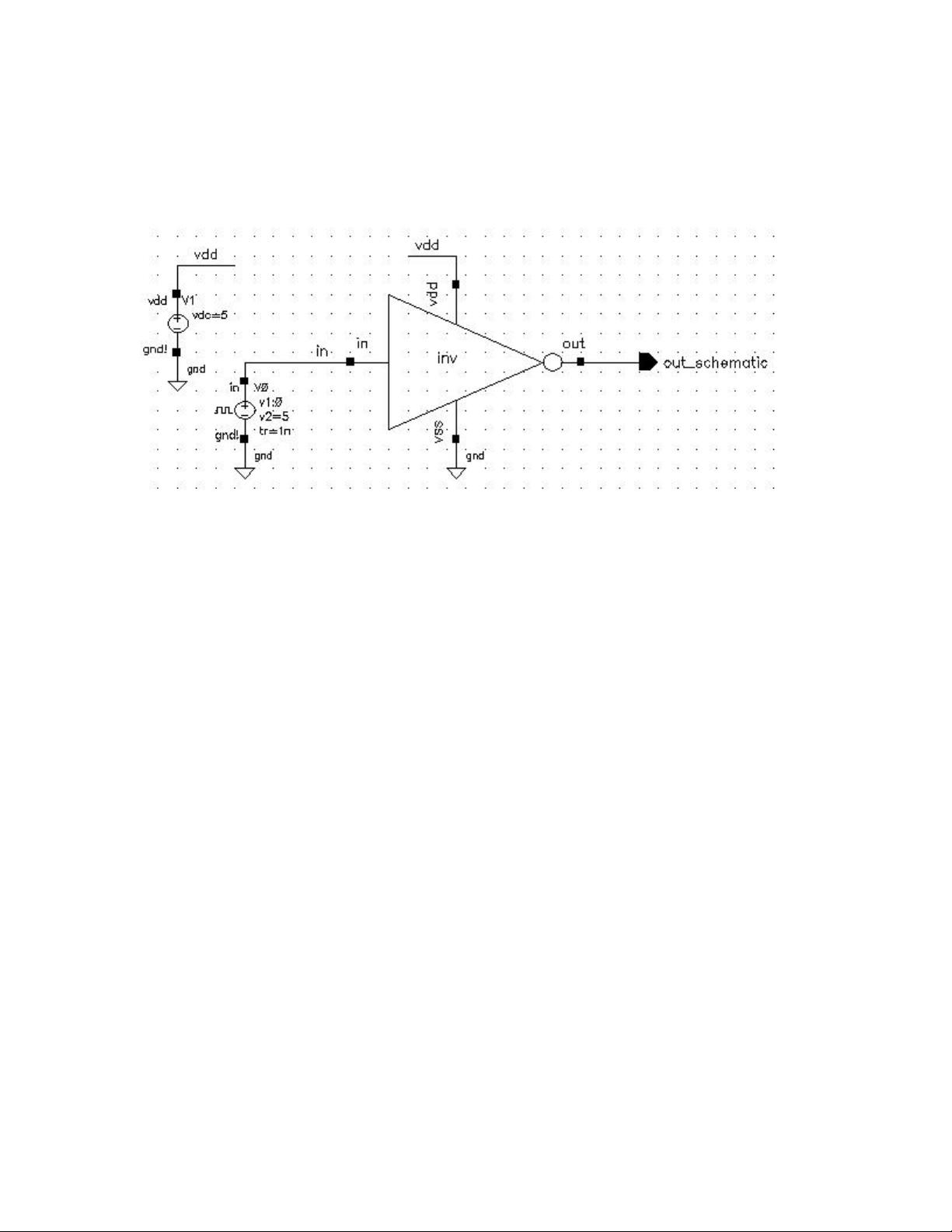
In this tutorial you’ll build an inverter in two different ways: as a schematic and as
layout. You know how to simulate the inverter using an analog simulator. After you
design and simulate the schematic, you will design layout for an inverter and simulate a
circuit extracted directly from the layout. You will be able to compare the two
simulations and see how they differ. You will also check the layout for design rules, and
check that the layout matches the schematic. Layout consists of the mask designs for
each layer that gets sent to the chip fabrication service.
Schematic:
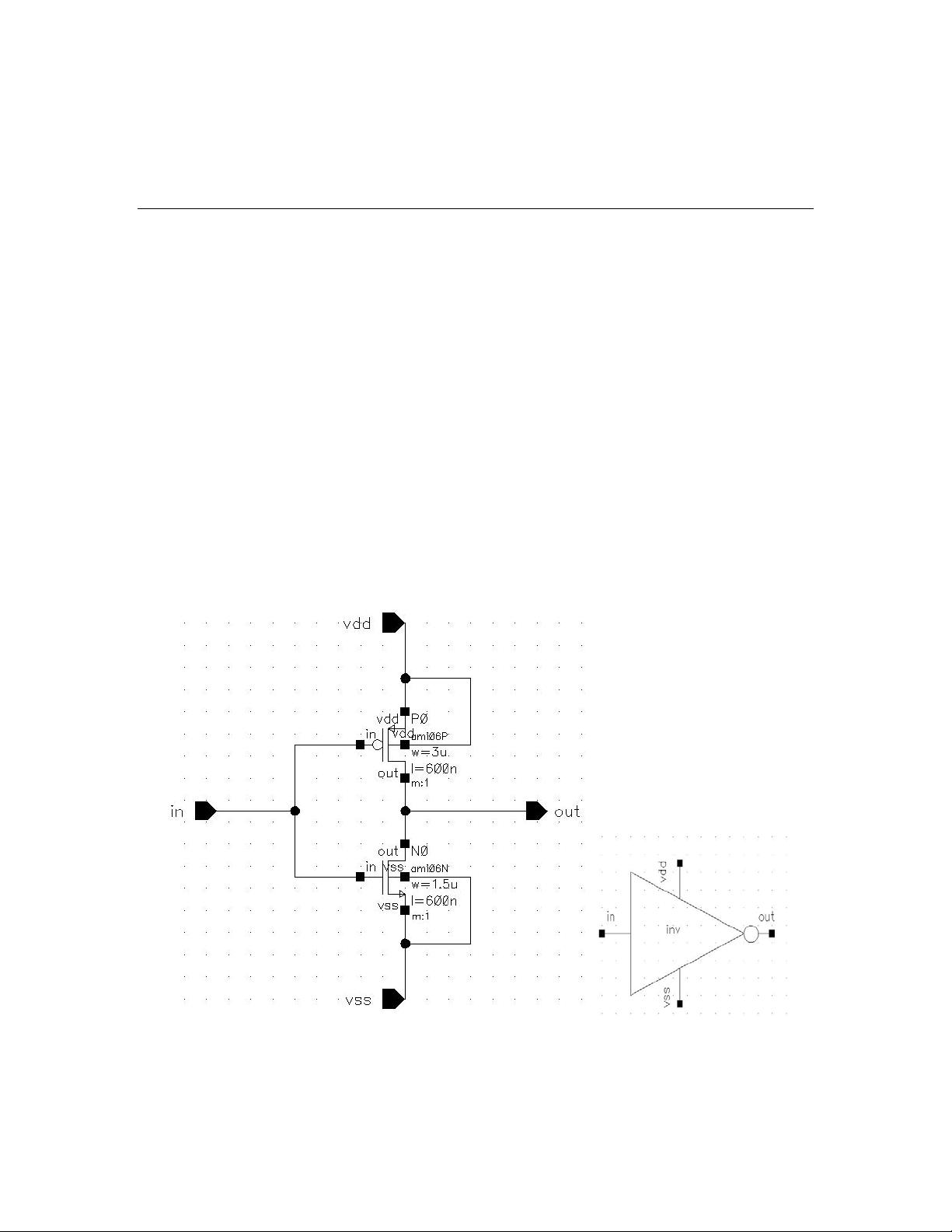
Draw the Schematic of an Inverter in Virtuoso Schematic Editor and make a
symbol.
Transistor Sizes: (W/L)
p
= 3.0/0.6 and (W/L)
n
= 1.5/0.6 (All in microns).
Body of pMOS is connected to Vdd and that of the nMOS is connected to Vss.
1


评论3