MediaTek Inc.
MT6139 Data Sheet
29 Sep, 2006
V2.0
PRELIMINARY, SUBJECT TO CHANGE WITHOUT NOTICE
3
MTK CONFIDENTIAL, NO DISCLOSURE
Table of contents
MT6139 Data Sheet................................................................................................................................................................. 1
Revision History...................................................................................................................................................................... 2
1 Introduction ................................................................................................................................................................... 4
1.1 Features.................................................................................................................................................................... 4
1.2 Applications .............................................................................................................................................................. 4
1.3 General Descriptions ................................................................................................................................................ 4
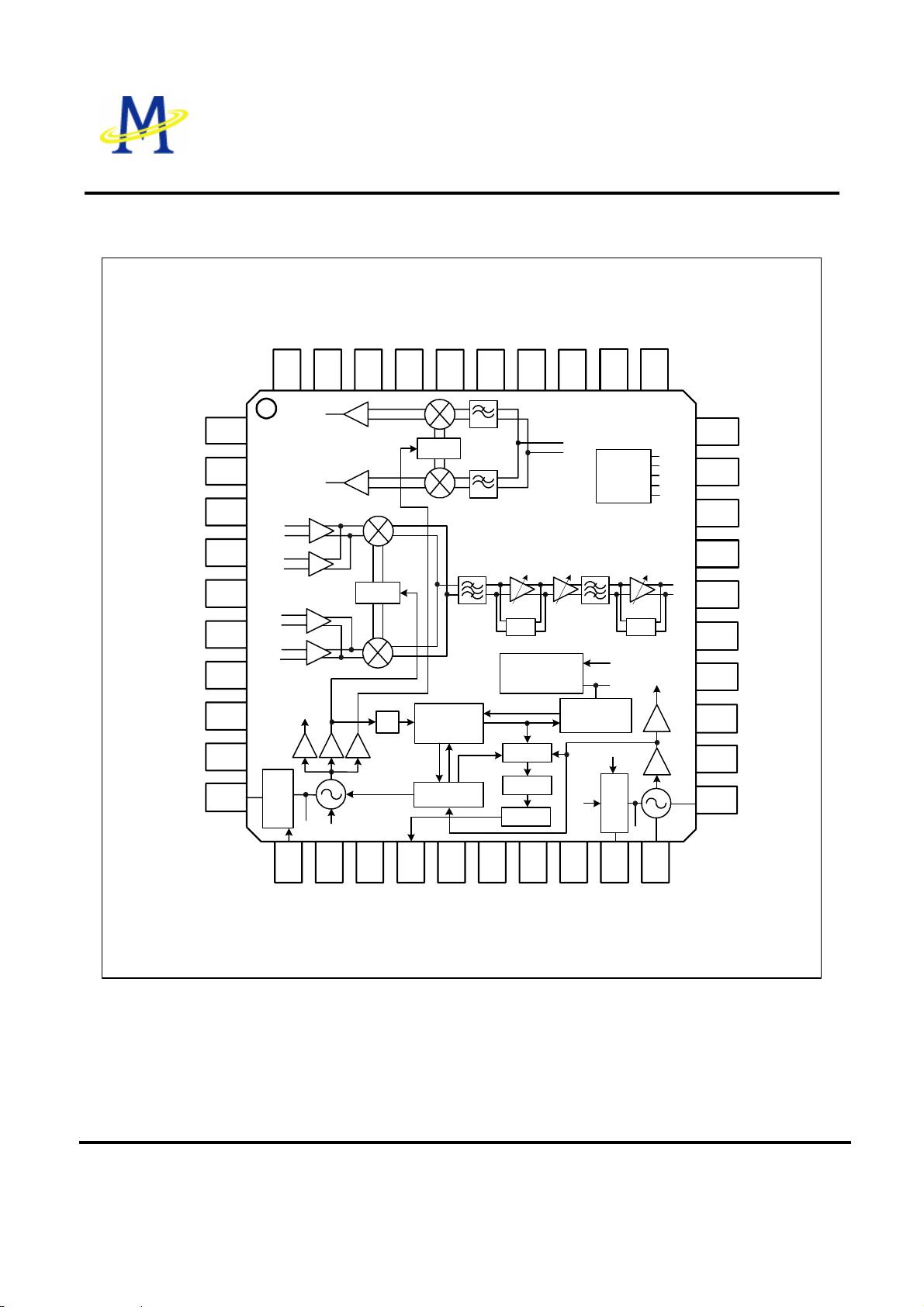
1.4 Functional Block Diagram......................................................................................................................................... 5
1.5 Pin Assignment and Description............................................................................................................................... 6
2 Functional Description ................................................................................................................................................. 7
2.1 Receiver.................................................................................................................................................................... 7
2.2 Transmitter................................................................................................................................................................ 7
2.3 RF Frequency Synthesizer ....................................................................................................................................... 7
2.3.1 Synthesizer System Description......................................................................................................................... 7
2.3.2 Synthesizer Frequency Programming ................................................................................................................ 8
2.3.3 Digital Frequency Calibration Loop .................................................................................................................... 8
2.3.4 Fast-Acquisition Option ...................................................................................................................................... 9
2.4 Voltage-Controlled Crystal Oscillator (VCXO) .......................................................................................................... 9
2.5 Regulator .................................................................................................................................................................. 9
3 MT6139 Hardware Control Pin Descriptions............................................................................................................. 10
4 Electrical Characteristics ........................................................................................................................................... 11
4.1 Absolute Maximum Ratings .................................................................................................................................... 11
4.2 Recommended Operating Range ........................................................................................................................... 11
4.3 DC Specifications ................................................................................................................................................... 12
5 Receiver Specifications.............................................................................................................................................. 13
6 Transmitter Specifications ......................................................................................................................................... 17
7 Frequency Synthesizer Specifications...................................................................................................................... 20
8 VCXO Specifications................................................................................................................................................... 21
9 Regulator Specifications ............................................................................................................................................ 22
9.1 Regulator 1 (SDM) Specifications........................................................................................................................... 22
9.2 Regulator 2 (VCO) Specifications........................................................................................................................... 22
9.3 Regulator 3 (VCXO) Specifications......................................................................................................................... 23
10 Package Dimensions .................................................................................................................................................. 24
11 Application Circuit ...................................................................................................................................................... 25
Bibliography References...................................................................................................................................................... 27