没有合适的资源?快使用搜索试试~ 我知道了~
资源推荐
资源详情
资源评论
VIA Telecom, Inc. Proprietary / Confidential Copyright © 2008 All Rights Reserved
The information in this document is believed to be correct at the time of writing, not printing.
VIA Telecom, Inc. reserves the right at any time to change said content, circuitry and specifications
CBP 7.0 Data Sheet
0700-0050-2a
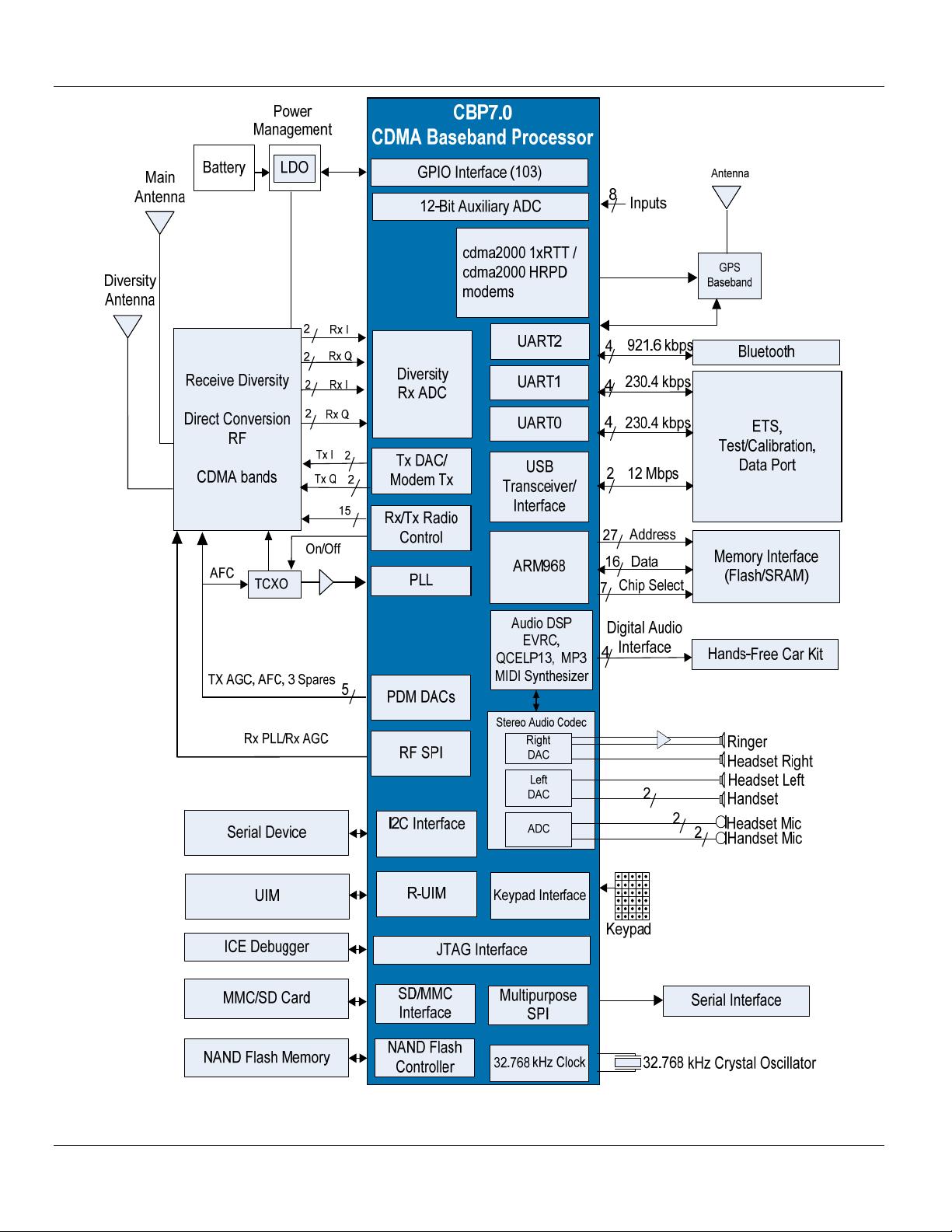
CBP 7.0 CDMA Baseband Processor
Features
• Single-chip CDMA baseband processor
• Supports cdma2000 1xRTT Release 0
• Supports cdma2000 HRPD Revision 0 and A
• Hybrid operation between 1x and HRPD
• Supports maximum data rates of
• 1xRTT: 153.6kbps for forward and reverse links
• HRPD: 3.1Mbps for forward link and 1.8Mbps for
reverse link
• ARM968E-S
®
Control Processor (CP) supports the protocol
stack, user interface, and hardware interface processing
• Two TeakLite® Digital Signal Processors (DSPs): one
supports CDMA modem processing, and the other supports
CDMA voice processing
• Supports multiple CDMA bands (Band Class 0/US-Cellular,
Band Class 1/US-PCS, Band Class 3/JTACS, Band Class
4/Korean-PCS); support for additional band classes as
defined in C.S0057-A can be added upon customer request
• Supports dual Rx Antenna Diversity
• Support for TCVCXO, VCXO and DCXO
• Mixed signal circuitry for the Rx analog-to-digital converter
(ADC), Rx Filter, Tx digital-to-analog converter (DAC), Tx
Filter, internal PLLs, voice codec (internal stereo DAC),
auxiliary DACs and ADC inputs, and 32.768 kHz oscillator
• RF control includes 4-wire RF SPI for controlling RF Rx and
Tx devices; 1.2288 to 19.6608 Mbps peak transfer rate and
dedicated RF control pins
• Includes I2C interface supporting 76.5 kbps to 1.288Mbps
peak transfer rate. Supports: reads and writes.
• Includes 3 UARTs, two of which operate at up to 230.4 kbps
and one of which operates at up to 921.6 kbps; each UART
can operate in IRDA mode at 153.2 kbps
• Support for an external application processor for performing
multimedia functions
• Supports an external GPS baseband processor
• Supports Universal Serial Bus 2.0 (USB 2.0) full mode,
including on-chip transceiver
• Removable User Identity Module (R-UIM) compliant with IS-
820
• 64-voice MIDI supporting 48 kHz sample rate and digital
ringer interface supporting I2S and PDM modes
• Supports interface to NAND Flash device for data storage
• MP3 decoder supports:
• MPEG I layer 3 decoding with sampling rate of 32,44.1,
or 48 KHz
• MPEG II layer 3 decoding with sampling rate of
16,22.05, or 24 kHz
• Enhanced file parser capable of handling MP3 bit
stream errors
• Supports burst/page mode memory accesses
• Seven chip selects and up to 27 address lines to access up
to 1.792 GB of external flash/SRAM
• Includes 4-wire multipurpose SPI which supports 244 kbps
to 31.25 Mbps peak transfer rate
• Supports interface to mass media devices in parallel or
serial modes
• Special purpose logic provides signal processing,
modulation, demodulation, hardware accelerators, and
interfaces for keypad and display
• Supports 6x4 or 6x5 keypad matrices and simultaneous
(dual) key press detection
• Capable of booting from internal ROM enabling
programming of flash through the UART pins
• Dual supply voltage (1.8 V digital core, 3.0 V analog and 3.0
V digital I/O)
• 3.0 V or 1.8 V external memory interface
CBP7.0 CDMA Baseband Processor Data Sheet
0700-0050-2a 2
VIA Telecom, Inc. Proprietary / Confidential Copyright © 2008 All Rights Reserved
The information in this document is believed to be correct at the time of writing, not printing.
VIA Telecom, Inc. reserves the right at any time to change said content, circuitry and specifications
Figure 1 Simplified Block Diagram of the CBP7.0 CDMA Baseband Processor
CBP7.0 CDMA Baseband Processor Data Sheet
0700-0050-2a 3
VIA Telecom, Inc. Proprietary / Confidential Copyright © 2008 All Rights Reserved
The information in this document is believed to be correct at the time of writing, not printing.
VIA Telecom, Inc. reserves the right at any time to change said content, circuitry and specifications
Table of Contents
Features............................................................................ 1
Description........................................................................ 5
CBP7.0 Hybrid Modem Features ...................................... 5
Hybrid access terminal operation .............................................5
cdma2000
®
1xRTT.................................................... 7
HRPD........................................................................ 7
Control Processor.....................................................................7
Digital Signal Processors..........................................................7
CBP7.0 Interface Description............................................ 7
Receive and Transmit Interfaces..............................................7
Receive Analog Interface.......................................... 7
Transmit Analog Interface......................................... 7
External Peripheral Interfaces ..................................................8
Power On/Off Interface ............................................. 8
Reset Interface.......................................................... 8
Clock Generation Interface ....................................... 8
TCXO Input Circuit/Phase Locked Loop (PLL)...... 8
32.768 kHz Oscillator Interface............................. 8
Analog and Digital Audio Interface ...........................................8
Analog Audio Interface.............................................. 8
Microphone Interface ............................................ 8
Analog Audio Input................................................ 8
Ringer Interface .................................................... 8
Digital Audio Interfaces ............................................. 8
External Digital Audio Interface............................. 8
I
2
S interface .......................................................... 9
PDM Interface....................................................... 9
CP External Memory Interface.................................................. 9
General Purpose Input/Output, Interrupt, and Output-Only
Interfaces ..............................................................................9
UART Ports...............................................................................9
USB ..........................................................................................9
Serial Peripheral Interface (SPI)...............................................9
RF SPI ...................................................................... 9
MSPI ....................................................................... 10
I2C Serial Interface .................................................................10
Removable User Identity Module (R-UIM) Interface...............10
Keypad and Display Interfaces...............................................10
Keypad Interface..................................................... 10
Display Interface ..................................................... 10
NAND Flash Interface............................................................. 10
SD Card/Mass Memory Card Interface................................... 10
Dedicated Radio Control Interface..........................................11
RF Power Control ................................................... 11
Transmitter Power Control ...................................... 11
RF PLL Lock ........................................................... 11
Pulse Density Modulated (PDM) Auxiliary DACs.................... 11
Auxiliary ADC.......................................................................... 11
External GPS Baseband.........................................................11
Mixed Signal Bias Circuits ...................................................... 11
Bandgap Reference Voltage................................... 11
Reference Currents................................................. 11
Common Mode Reference Voltage......................... 11
Test and Debug Interfaces .....................................................11
JTAG Interface........................................................ 11
Auxiliary Clock Output .............................................11
Development Tools .................................................................11
CDS7.......................................................................11
ETS .........................................................................12
Product Documentation ..........................................................12
Signal Listing Sorted by Ball Number).....................11
Signal Listing (Sorted by Signal Name)...................15
Software Features and Functions....................................18
Industry-Standard Features and Functions.............................18
Additional Software Functions ................................................19
Software Architecture ......................................................20
Software Application Programming Interfaces (APIs).............20
User Interface-VIA Abstraction Layer (UI-VAL) API 20
VAL-CP API.............................................................21
Layer One API (L1 API)...........................................21
System Services API...............................................21
CP/DSP API ............................................................21
Hardware API (HW API)..........................................21
Software Modules Description ................................................21
UI.............................................................................21
VAL .........................................................................21
Protocol Stack Engine and Wrapper .......................21
Service Configuration Controller (SCC)...................21
Application Interface Wrapper (AIW).......................21
High Layer Wrapper (HLW).....................................21
Radio Link Protocol (RLP).......................................21
Layer 1 ....................................................................21
Multiplexed Sublayer ...............................................21
Database Manager (DBM).......................................21
Monitor and Diagnostics (MON) ..............................21
Inter-Processor Communication (IPC).....................21
System Services (SYS) ...........................................21
Hardware Drivers (HWD).........................................22
Input Output (IOP)...................................................22
Executive (EXE) Wrapper (RTOS) ..........................22
Typical Current Consumption..........................................22
Package Drawing – Top View .................................23
Package Drawing – Bottom View ............................24
Solder Reflow Profile (Lead-Containing Packages).25
Recommended Pad Diameter Dimensions for Printed
Circuit Board............................................................25
Pad Dimensions ..................................................25
Appendix A: Pin-out Information.............................26
Ordering Information ...............................................32
References......................................................................32
CBP7.0 CDMA Baseband Processor Data Sheet
0700-0050-2a 4
VIA Telecom, Inc. Proprietary / Confidential Copyright © 2008 All Rights Reserved
The information in this document is believed to be correct at the time of writing, not printing.
VIA Telecom, Inc. reserves the right at any time to change said content, circuitry and specifications
Table of Figures
Figure 1 Simplified Block Diagram of the CBP7.0 CDMA
Baseband Processor 2
Figure 2 CBP7.0 High-Level Software Architecture 20
Figure 3 Solder Reflow 26 °C Profile for Lead-Containing
Package 25
Figure 4 Recommended Pad Diameter Dimensions for PC
Board 25
Table of Tables
Table 1 3GPP2 Service Options Supported by CBP7.0
Software 18
Table 2 Proprietary Service Options Supported by CBP7.0
Software 19
Table 3 Additional Supported Software Features 19
Table 4 – CBP7.0 CDMA Current Consumption 22
CBP7.0 CDMA Baseband Processor Data Sheet
0700-0050-2a 5
VIA Telecom, Inc. Proprietary / Confidential Copyright © 2008 All Rights Reserved
The information in this document is believed to be correct at the time of writing, not printing.
VIA Telecom, Inc. reserves the right at any time to change said content, circuitry and specifications
Description
VIA Telecom’s single-chip CDMA Baseband Processor
7.0 (CBP7.0) provides a hybrid solution that supports
3G cdma2000
®
1xRTT (Release 0) and HRPD
(Revision A). It is designed to meet or exceed the
specifications of mobile stations for worldwide 3G
CDMA systems as specified by IS-2000 1xRTT
(Release 0), & IS-856-A standards and is backward-
compatible to IS-95. It also includes support for an
external GPS baseband modem.
The CBP7.0 integrates mixed signal, analog, and digital
functions with a seamless interface to multiple RF
solutions from the industry’s leading suppliers. This
flexibility enables faster design cycles and reduces the
overall mobile station cost. Additionally, CBP7.0 is
manufactured using an industry-standard low power
CMOS process with multi-foundry support for security
of supply.
CBP7.0 Hybrid Modem Features
The CBP7.0 Hybrid Modem is designed to allow
operation in both cdma2000 1xRTT and HRPD
networks, and is able to hand off between them as
required to support the services provided by both types
of networks.
The CBP7.0 uses a Preferred Roaming List (PRL) and
a System Acquisition Preference that allows the user to
select between 3 system types for initial network
acquisition. These options can be configured on the fly
and the acquisition preference is stored in nonvolatile
memory.
Hybrid access terminal operation
• Hybrid (1xRTT and HRPD)
• Voice preferred HRPD + cdma2000 1x hybrid
• Data preferred HRPD + cdma2000 1x hybrid
• cdma2000 1xRTT only
• HRPD only
cdma2000
1xRTT
Operation
Power-Up
Hybrid
Operation
System Acquisition Preference
== Hybrid
System Acquisition Preference
== 1xRTT Only
HRPD
Operation
System Acquisition Preference
== HRPD Only
System Acquisition Preference
== Hybrid
System Acquisition Preference
== 1xRTT Only
System Acquisition Preference
== HRPD Only
System Acquisition Preference
== Hybrid
剩余34页未读,继续阅读
资源评论
- zhaoweicpp2014-12-26不错 资料挺好
- qetuoadgj2016-10-21挺詳細的資料,感謝
- jeff-dong2012-06-18刚准备用这款芯片,资料挺好的。
sunriseye
- 粉丝: 1
- 资源: 35
上传资源 快速赚钱
- 我的内容管理 展开
- 我的资源 快来上传第一个资源
- 我的收益 登录查看自己的收益
- 我的积分 登录查看自己的积分
- 我的C币 登录后查看C币余额
- 我的收藏
- 我的下载
- 下载帮助
最新资源
- 论文(最终)_20240430235101.pdf
- 基于python编写的Keras深度学习框架开发,利用卷积神经网络CNN,快速识别图片并进行分类
- 最全空间计量实证方法(空间杜宾模型和检验以及结果解释文档).txt
- 5uonly.apk
- 蓝桥杯Python组的历年真题
- 2023-04-06-项目笔记 - 第一百十九阶段 - 4.4.2.117全局变量的作用域-117 -2024.04.30
- 前端开发技术实验报告:内含4四实验&实验报告
- Highlight Plus v20.0.1
- 林周瑜-论文.docx
资源上传下载、课程学习等过程中有任何疑问或建议,欢迎提出宝贵意见哦~我们会及时处理!
点击此处反馈
安全验证
文档复制为VIP权益,开通VIP直接复制
信息提交成功