COMPANY CONFIDENTIAL • 1
Data Sheet
© 2010 by Atheros Communications, Inc. All rights reserved. Atheros®, Atheros Driven®, Align®, Atheros XR®, Driving the Wireless Future®, Intellon®, Ethos®, IQUE®,
No New Wires®, Orion®, PLC4Trucks®, Powerpacket®, Spread Spectrum Carrier®, SSC®, ROCm®, Super A/G®, Super G®, Super N®, The Air is Cleaner at 5-GHz®, Total
802.11®, U-Nav®, Wake on Wireless®, Wireless Future. Unleashed Now.®, and XSPAN®, are registered by Atheros Communications, Inc. Atheros SST™, Signal-Sustain
Technology™, Install N Go™, ROCm™, amp™, Simpli-Fi™, There is Here™, U-Map™, U-Tag™, and 5-UP™ are trademarks of Atheros Communications, Inc. The Atheros
logo is a registered trademark of Atheros Communications, Inc. All other trademarks are the property of their respective holders. Subject to change without notice.
PRELIMINARY
December 2010
AR9344 Highly-Integrated and Feature-Rich IEEE 802.11n 2x2
2.4/5 GHz Premium SoC for Advanced WLAN Platforms
General Description
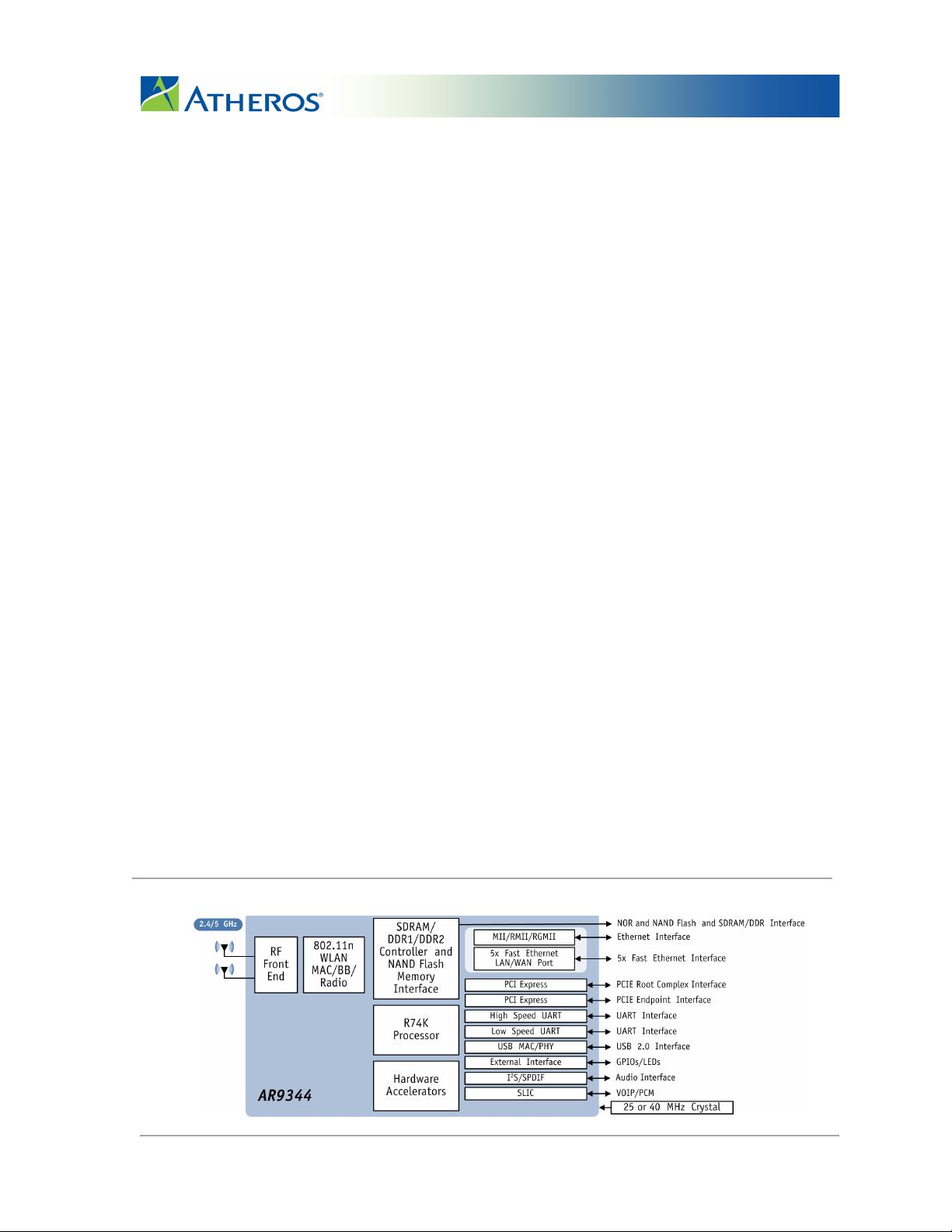
The Atheros AR9344 is a highly integrated and
feature-rich IEEE 802.11n 2x2 2.4/5 GHz System-
on-a-Chip (SoC) for advanced WLAN platforms.
It includes a MIPS 74Kc processor, PCI Express
1.1 Root Complex and Endpoint interfaces, five
port IEEE 802.3 Fast Ethernet Switch with MAC/
PHY, one MII/RMII/RGMII interface, one USB
2.0 MAC/PHY, and external memory interface
for serial Flash, SDRAM, DDR1 or DDR2, I
2
S/
SPDIF-Out audio interface, SLIC VOIP/PCM
interface, two UARTs, and GPIOs that can be
used for LED controls or other general purpose
interface configurations.
The AR9344 supports 802.11n operations up to
144 Mbps for 20 MHz and 300 Mbps for 40 MHz
respectively, and 802.11a/b/g data rates.
Additional features include Maximal Likelihood
(ML) decoding, Low-Density Parity Check
(LDPC), Maximal Ratio Combining (MRC), Tx
Beamforming (TxBF), and On-Chip One-Time
Programmable (OTP) memory.
The AR9344 PCIE Root Complex interface can be
used to connect to another Atheros single-chip
MAC/BB/radio for dual concurrent WLAN
applications. The AR9344 supports booting from
either NOR or NAND flash. If NOR flash is used
as boot codestore, an additional NAND flash
device can still be connected, for end-user multi-
media storage and other applications.
When connecting the AR9344 to an external host
through the PCIE Endpoint interface, or the USB
Device interface, the AR9344 can off load the host
CPU from computation- intensive functions,
allowing it to focus on its dedicated tasks.
Features
■ 74Kc MIPS processor with 64 KB I-Cache and
32 KB D-Cache, operating at up to 533 MHz
■ External 16- or 32-bit DDR1, DDR2 operating
at up to 200 MHz (400 M transfers/sec), or 16-
bit SDRAM memory interface operating at up
to 200 MHz
■ NAND and SPI NOR Flash memory support
■ 10/100 Ethernet Switch with five IEEE 802.3
Ethernet LAN ports
■ MII/RMII/RGMII interface
■ 802.3az Energy Efficient Ethernet compliant
■ Hardware-based NAT & ACL accelerators for
Ethernet interface
■ Both PCI Express 1.1 Root Complex and
Endpoint interfaces supported
simultaneously
■ One USB 2.0 controller with built-in MAC/
PHY supports Host or Device mode
■ Boot from external CPU via PCIE, USB, xMII,
eliminating need for external flash
■ I
2
S/SPDIF-out audio interface
■ SLIC for VOIP/PCM
■ One low-speed UART (115 Kbps), one high-
speed UART (3 Mbps), and multiple GPIO
pins for general purpose I/O
■ Fully integrated RF Front-End including PAs
and LNAs
■ Optional external LNA/PA
■ 25 MHz or 40 MHz reference clock input
■ 1.2 V switching regulator
■ Advanced power management with dynamic
clock switching for ultra-low power modes
■ 409-pin BGA package
AR9344 System Block Diagram


 我的内容管理
展开
 我的资源
快来上传第一个资源
 我的收益 登录查看自己的收益
 我的积分
登录查看自己的积分
 我的C币
登录后查看C币余额
 我的收藏
我的收藏  我的下载
我的下载  下载帮助
下载帮助 
 前往需求广场,查看用户热搜

 信息提交成功