没有合适的资源?快使用搜索试试~ 我知道了~
lecture03-151116.pdf
需积分: 5 0 下载量 92 浏览量
2023-10-25
08:24:13
上传
评论
收藏 2MB PDF 举报
温馨提示
![preview](https://dl-preview.csdnimg.cn/88469235/0001-93b9024099ec2d793b254eee800bdc90_thumbnail.jpeg)
![preview-icon](https://csdnimg.cn/release/downloadcmsfe/public/img/scale.ab9e0183.png)
试读
27页
lecture03-151116
资源推荐
资源详情
资源评论
![pdf](https://img-home.csdnimg.cn/images/20210720083512.png)
![zip](https://img-home.csdnimg.cn/images/20210720083736.png)
![pdf](https://img-home.csdnimg.cn/images/20210720083512.png)
![](https://csdnimg.cn/release/download_crawler_static/88469235/bg1.jpg)
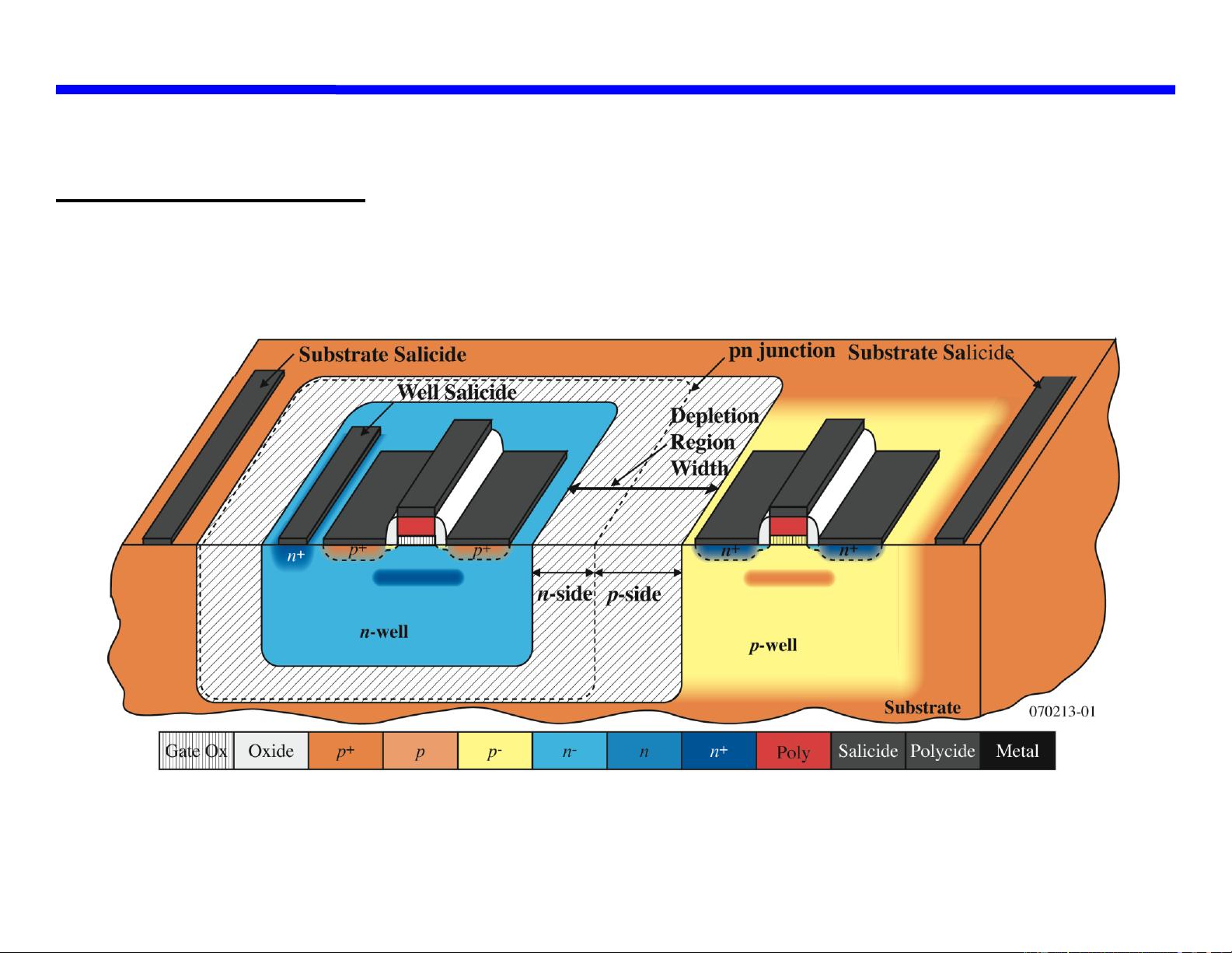
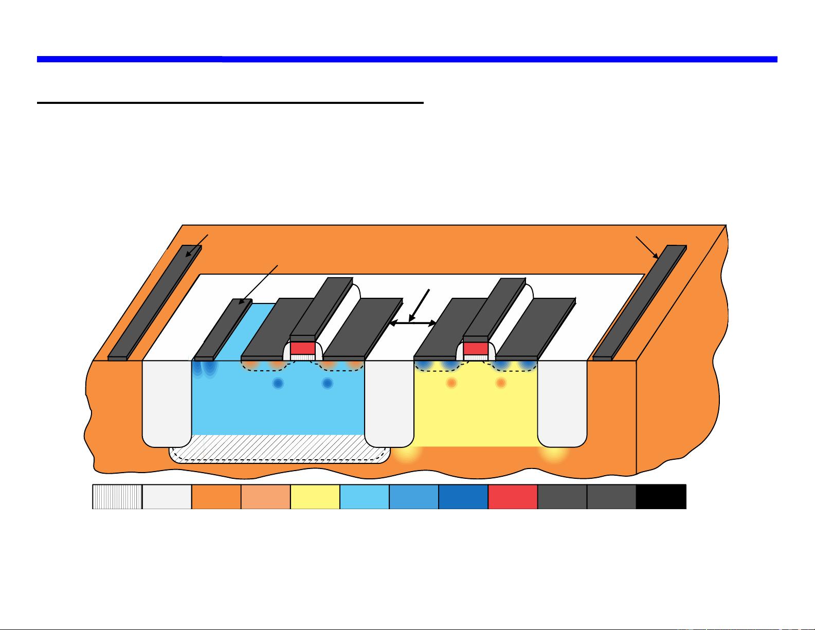
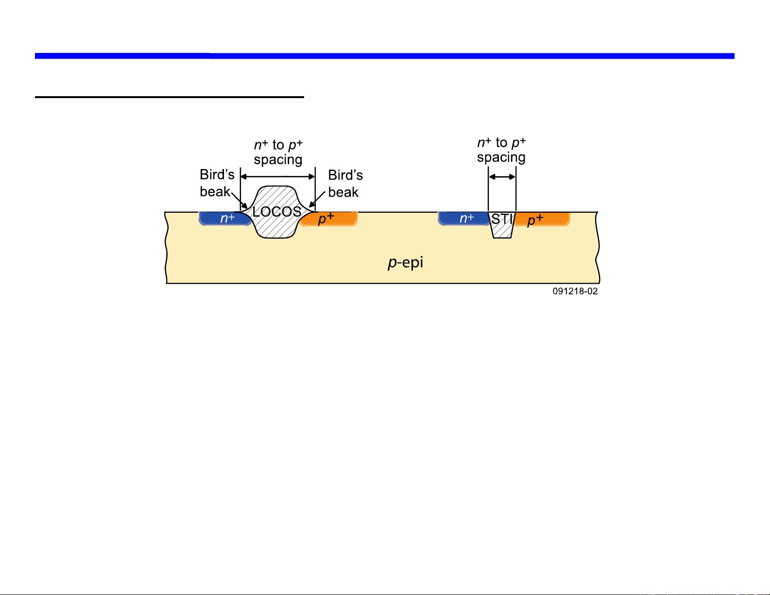
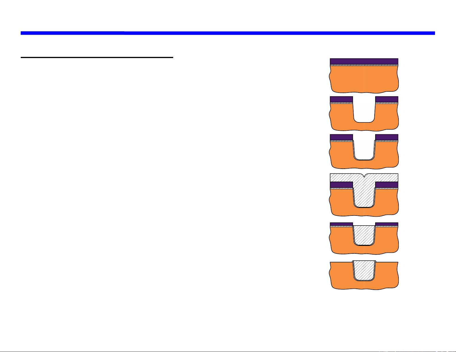
Lecture 03 – DSM CMOS Technology (11/16/15) Page 03-1
CMOS Analog Circuit Design © P.E. Allen - 2016
LECTURE 03 - DEEP SUBMICRON (DSM) CMOS TECHNOLOGY
LECTURE ORGANIZATION
Outline
• Characteristics of a deep submicron CMOS technology
• Typical deep submicron CMOS technology
• Summary
CMOS Analog Circuit Design, 3
rd
Edition Reference
New material
![](https://csdnimg.cn/release/download_crawler_static/88469235/bg2.jpg)
Lecture 03 – DSM CMOS Technology (11/16/15) Page 03-2
CMOS Analog Circuit Design © P.E. Allen - 2016
CHARACTERISTICS OF A DEEP SUBMICRON CMOS TECHNOLOGY
Isolation of Transistors
The use of reverse bias pn junctions to isolate transistors becomes impractical as the
transistor sizes decrease.
![](https://csdnimg.cn/release/download_crawler_static/88469235/bg3.jpg)
Lecture 03 – DSM CMOS Technology (11/16/15) Page 03-3
CMOS Analog Circuit Design © P.E. Allen - 2016
Use of Shallow Trench Isolation Technology
Shallow trench isolation (STI) allows closer spacing of transistors by eliminating the
depletion region at the surface.
p
+
pp
-
MetalSalicide
n
-
n n
+
Oxide
Poly
070330-03
Polycide
Gate Ox
n
+
n-well
n
+
p-well
n
+
Substrate
n
+
Shallow
Trench
Isolation
n
+
Shallow
Trench
Isolation
Shallow
Trench
Isolation
p
+
p
+
n
+
n
+
Substrate Salicide
Well Salicide
Decreased
spacing
Substrate Salicide
S
h
a
l
l
o
w
Trench Isolation
I
s
o
l
a
t
i
o
n
S
h
a
l
l
o
w
T
r
e
n
c
h
![](https://csdnimg.cn/release/download_crawler_static/88469235/bg4.jpg)
Lecture 03 – DSM CMOS Technology (11/16/15) Page 03-4
CMOS Analog Circuit Design © P.E. Allen - 2016
Comparison of STI and LOCOS
What are the differences between a LOCOS and STI technology?
Comments:
• If the n
+
to p
+
spacing is large, the Bird’s beak can be compensated using techniques
such as poly buffered LOCOS
• At some point as the n
+
to p
+
spacing gets smaller, the restricted bird’s beak leads to
undesirable stress effects in the transistor.
• An important advantage of STI is that it minimizes the heat cycle needed for n
+
or p
+
isolation compared to LOCOS. This is a significant advantage for any process where
there are implants before STI.
![](https://csdnimg.cn/release/download_crawler_static/88469235/bg5.jpg)
Lecture 03 – DSM CMOS Technology (11/16/15) Page 03-5
CMOS Analog Circuit Design © P.E. Allen - 2016
Shallow Trench Isolation (STI)
060203-01
Nitride
Silicon
(1)
(2)
(3)
(4)
(5)
(6)
1.) Cover the wafer with pad oxide and silicon nitride.
2.) First etch nitride and pad oxide. Next, an anisotropic
etch is made in the silicon to a depth of 0.4 to 0.5 microns.
3.) Grow a thin thermal oxide layer on the trench walls.
4.) A CVD dielectric film is used to fill the trench.
5.) A chemical mechanical polishing (CMP) step is used to
polish back the dielectric layer until the nitride is reached.
The nitride acts like a CMP stop layer.
6.) Densify the dielectric material at 900°C and strip the
nitride and pad oxide.
剩余26页未读,继续阅读
资源评论
![avatar-default](https://csdnimg.cn/release/downloadcmsfe/public/img/lazyLogo2.1882d7f4.png)
![avatar](https://profile-avatar.csdnimg.cn/default.jpg!1)
学海泛舟吖
- 粉丝: 0
- 资源: 178
上传资源 快速赚钱
我的内容管理 展开
我的资源 快来上传第一个资源
我的收益
登录查看自己的收益我的积分 登录查看自己的积分
我的C币 登录后查看C币余额
我的收藏
我的下载
下载帮助
![voice](https://csdnimg.cn/release/downloadcmsfe/public/img/voice.245cc511.png)
![center-task](https://csdnimg.cn/release/downloadcmsfe/public/img/center-task.c2eda91a.png)
最新资源
- vs 2019 c++20规范 S TL库中的 ratio duration<T,U> time-point<T,U>等
- Idea哈哈哈哈哈哈哈哈哈
- vs 2019 c++20 规范的头文件 <future> 源码注释和几个结论
- vs 2019 c++20规范 S TL 库中头文件 <atomic> 源码注释及探讨几个知识点
- c++20 规范, v s 2019 , 头文件 <m u t ex > ,注释以及几个探讨
- ED247-LIBRARY,V2.0.1,V2.3.0
- 一个简单的Vue应用的创建过程
- 10_QQ浏览器压缩包.zip
- 超外差式接收器设计.zip
- 11-checkpoint.ipynb
资源上传下载、课程学习等过程中有任何疑问或建议,欢迎提出宝贵意见哦~我们会及时处理!
点击此处反馈
![feedback](https://img-home.csdnimg.cn/images/20220527035711.png)
![feedback-tip](https://img-home.csdnimg.cn/images/20220527035111.png)
安全验证
文档复制为VIP权益,开通VIP直接复制
![dialog-icon](https://csdnimg.cn/release/downloadcmsfe/public/img/green-success.6a4acb44.png)