没有合适的资源?快使用搜索试试~ 我知道了~
资源推荐
资源详情
资源评论
May 1997
ML2258*
µP Compatible 8-Bit A/D Converter
with 8-Channel Multiplexer
1
GENERAL DESCRIPTION
The ML2258 combines an 8-bit A/D converter, 8-channel
analog multiplexer, and a microprocessor compatible 8-
bit parallel interface and control logic in a single
monolithic device.
Easy interface to microprocessors is provided by the
latched and decoded multiplexer address inputs and
latched three-state outputs.
The device is suitable for a wide range of applications
from process and machine control to consumer,
automotive, and telecommunication applications.
The ML2258 is an enhanced, pin-compatible, second
source for the industry standard ADC0808/ADC0809. The
ML2258 enhancements are faster conversion time, true
sample and hold function, superior power supply
rejection, wider reference range, and a double buffered
data bus as well as faster digital timing. All parameters
are guaranteed over temperature with a power supply
voltage of 5V ±10%.
FEATURES
■ Conversion time 6.6µs
■ Total unadjusted error ±1/2LSB or ±1LSB
■ No missing codes
■ Sample and hold 390ns acquisition
■ Capable of digitizing a 5V, 50kHz sine wave
■ 8-input multiplexer
■ 0V to 5V analog input range with single 5V
power supply
■ Operates ratiometrically or with up to 5V
voltage reference
■ No zero-or full-scale adjust required
■ Analog input protection 25mA per input min
■ Low power dissipation 3mA max
■ TTL and CMOS compatible digital inputs and outputs
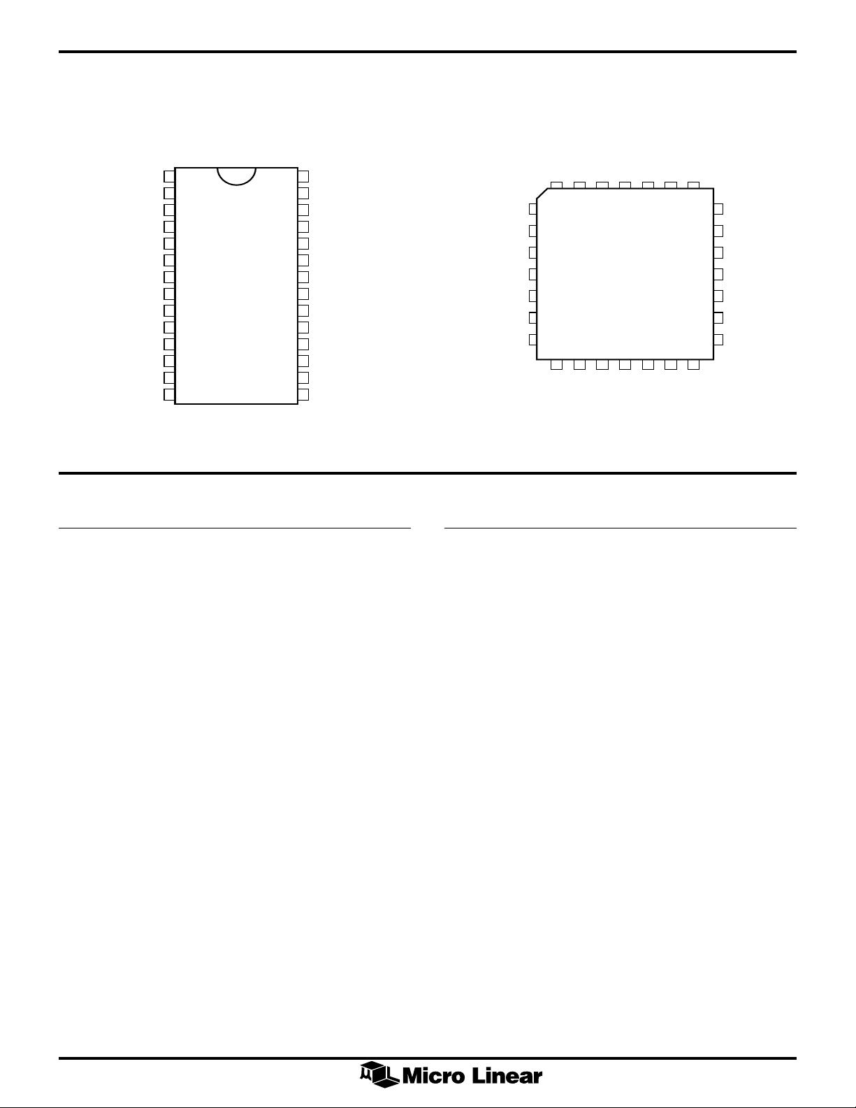
■ Standard 28-pin DIP or surface mount PCC
■ Superior pin compatible replacement for ADC0808 and
ADC0809
* Some Packages Are End Of Life As Of August 1, 2000
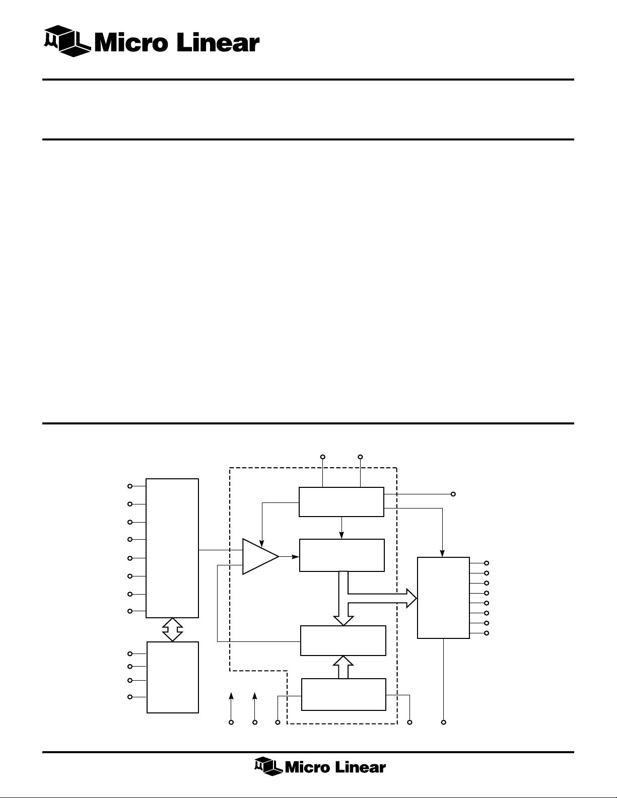
BLOCK DIAGRAM
COMPARATOR
A/D WITH
SAMPLE HOLD
CONTROL & TIMING
S.A.R.
SWITCH TREE
THREE
STATE
OUTPUT
LATCH
BUFFER
DB0
DB1
DB2
DB3
DB4
DB5
DB6
DB7
OUTPUT
ENABLE
–V
REF
+V
REF
GNDV
CC
CAPACITOR/
RESISTOR
ARRAY
ADDRESS
LATCH
AND
DECODER
ADDR0
ADDR1
ADDR2
ADDRESS
LATCH ENABLE
IN7
IN6
IN0
IN1
IN2
IN3
IN4
IN5
8-CHANNEL
MULTIPLEXER
START CLOCK
END OF CONVERSION
(INTERRUPT)
ML2258
2
PIN CONFIGURATION
ML2258
28-Pin DIP (P28)
ML2258
28-Pin PCC (Q28)
IN3
IN4
IN5
IN6
IN7
START
EOC
DB3
OE
CLK
V
CC
+V
REF
GND
DB1
IN2
IN1
IN0
ADDR0
ADDR1
ADDR2
ALE
DB7
DB6
DB5
DB4
DB0
–V
REF
DB2
1
2
3
4
5
6
7
8
9
10
11
12
13
14
28
27
26
25
24
23
22
21
20
19
18
17
16
15
TOP VIEW
PIN DESCRIPTION
PIN# NAME FUNCTION
1 IN3 Analog input 3.
2 IN4 Analog input 4.
3 IN5 Analog input 5.
4 IN6 Analog input 6.
5 IN7 Analog input 7.
6 START Start of conversion. Active high digital
input pulse initiates conversion.
7 EOC End of conversion. This output goes
low after a START pulse occurs, stays
low for the entire A/D conversion, and
goes high after conversion is
completed. Data on DB0–DB7 is valid
on rising edge of EOC and stays valid
until next EOC rising edge.
8 DB3 Data output 3.
9 OE Output enable input. When OE = 0,
DB0–DB7 are in high impedance
state; OE = 1, DB0–DB7 are active
outputs.
10 CLK Clock. Clock input provides timing for
A/D converter, S/H, and digital
interface.
11 V
CC
Positive supply. 5V ± 10%.
12 +V
REF
Positive reference voltage.
PIN# NAME FUNCTION
13 GND Ground. 0V, all analog and digital
inputs or outputs are reference to this
point.
14 DB1 Data output 1.
15 DB2 Data output 2.
16 –V
REF
Negative reference voltage.
17 DB0 Data output 0.
18 DB4 Data output 4.
19 DB5 Data output 5.
20 DB6 Data output 6.
21 DB7 Data output 7.
22 ALE Address latch enable. Input to latch in
the digital address (ADDR2–0) on the
rising edge of the multiplexer.
23 ADDR0 Address input 0 to multiplexer. Digital
input for selecting analog input.
24 ADDR1 Address input 1 to multiplexer. Digital
input for selecting analog input.
25 ADDR2 Address input 2 to multiplexer. Digital
input for selecting analog input.
26 IN0 Analog input 0.
27 IN1 Analog input 1.
28 IN2 Analog input 2.
ADDR0
ADDR1
ADDR2
ALE
DB7
DB6
DB5
IN7
START
EOC
DB3
OE
CLK
V
CC
12 13 14 15 16
IN6
IN5
IN4
IN3
IN2
IN1
IN0
+V
REF
GND
DB1
DB2
–V
REF
DB0
DB4
17 18
5
6
7
8
9
10
11
432128
25
24
23
22
21
20
19
27 26
TOP VIEW
ML2258
3
ELECTRICAL CHARACTERISTICS
Unless otherwise specified, T
A
= T
MIN
to T
MAX
, V
CC
= +V
REF
= 5V ±10%, –V
REF
= GND and f
CLK
= 10.24MHz
ML2258B ML2258C
TYP TYP
PARAMETER NOTES CONDITIONS MIN (NOTE 4) MAX MIN (NOTE 4) MAX UNITS
Converter and Multiplexer
Total Unadjusted Error 5, 7 V
REF
= V
CC
±1/2 ±1 LSB
+V
REF
Voltage Range 6 –V
REF
V
CC
+ 0.1 –V
REF
V
CC
+ 0.1 V
–V
REF
Voltage Range 6 GND – 0.1 +V
REF
GND – 0.1 +V
REF
V
Reference Input Resistance 5 14 20 28 14 20 28 k ý
Analog Input Range 5, 8 GND – 0.1 V
CC
+ 0.1 GND – 0.1 V
CC
+ 0.1 V
Power Supply Sensitivity 6 DC, V
CC
= 5V ± 10% ±1/32 ±1/4 ±1/32 ±1/4 LSB
100mVp-p, 100kHz ±1/16 ±1/16 LSB
sine on V
CC
, V
IN
= 0
I
OFF
, Off Channel Leakage 5, 9 On Channel = V
CC
–1 –1 µA
Current (Note 9) Off Channel = 0V
On Channel = 0V 1 1 µA
Off Channel = V
CC
I
ON
, On Channel Leakage 5, 9 On Channel = 0V –1 –1 µA
Current (Note 9) Off Channel = V
CC
On Channel = V
CC
11µA
Off Channel = 0V
Digital and DC
V
IN(1)
, Logical “1” Input 5 2.0 2.0 V
Voltage
V
IN(0)
, Logical “0” Input 5 0.8 0.8 V
Voltage
I
IN(1)
, Logical “1” Input 5 V
IN
= V
CC
11µA
Current
I
IN(0)
, Logical “0” Input 5 V
IN
= 0V –1 –1 µA
Current
V
OUT(1)
, Logical “1” 5 I
OUT
= –2mA 4.0 4.0 V
Output Voltage
V
OUT(0)
, Logical “0” 5 I
OUT
= 2mA 0.4 0.4 V
Output Voltage
I
OUT
, Three-State Output 5 V
OUT
= 0V –1 –1 µA
Current V
OUT
= V
CC
11µA
I
CC
, Supply Current 5 1.5 3 1.5 3 mA
ABSOLUTE MAXIMUM RATINGS
(Note 1)
Supply Voltage, V
CC
.............................................................. 6.5V
Voltage
Logic Inputs .................................. –0.3V to V
CC
+0.3V
Analog Inputs ............................... –0.3V to V
CC
+0.3V
Input Current per Pin (Note 2) ..............................±25mA
Storage Temperature ..............................–65°C to +150°C
Package Dissipation
at T
A
= 25°C (Board Mount) .............................875mW
Lead Temperature (Soldering 10 sec.)
Dual-In-Line Package (Plastic)............................ 260°C
Molded Chip Carrier Package
Vapor Phase (60 sec.) ..................................... 215°C
Infrared (15 sec.) ............................................ 220°C
OPERATING CONDITIONS
Supply Voltage, V
CC
.................................... 4.5V
DC
to 6.3V
DC
Temperature Range (Note 3) ................. T
MIN
- T
A
- T
MAX
ML2258BIP, ML2258BIQ, ML2258CIP,
ML2258CIQ ........................................–40°C to +85°C
剩余11页未读,继续阅读
资源评论
普通网友
- 粉丝: 0
- 资源: 1
上传资源 快速赚钱
- 我的内容管理 展开
- 我的资源 快来上传第一个资源
- 我的收益 登录查看自己的收益
- 我的积分 登录查看自己的积分
- 我的C币 登录后查看C币余额
- 我的收藏
- 我的下载
- 下载帮助
安全验证
文档复制为VIP权益,开通VIP直接复制
信息提交成功