NE6510179Adetashaeet
需积分: 5 102 浏览量
2022-09-14
11:41:32
上传
评论
收藏 277KB PDF 举报

NEC's 3W, L&S-BAND
MEDIUM POWER GaAs HJ-FET
FEATURES
• LOW COST PLASTIC SURFACE MOUNT PACKAGE
Available on Tape and Reel
• USABLE TO 3.7 GHz:
Fixed Wireless Access, ISM, WLL, MMDS, IMT-2000,
PCS
• HIGH OUTPUT POWER:
35 dBm TYP with 5.0 V Vdc
32.5 dBm TYP with 3.5 V Vdc
• HIGH LINEAR GAIN:
10 dB TYP at 1.9 GHz
• LOW THERMAL RESISTANCE:
5°C/W
NE6510179A
DESCRIPTION
NEC's NE6510179A is a GaAs HJ-FET designed for medium
power mobile communications, Fixed Wireless Access, ISM,
WLL, PCS, IMT-2000, and MMDS transmitter and subscriber
applications. It is capable of delivering 1.8 watts of output
power(C/W) at 3.5 V and 3 Watts of ouptut power (CW) at 5 V
with high linear gain, high efficiency, and excellent linearity.
Reliability and performance uniformity are assured by NEC's
stringent quality and control procedures.
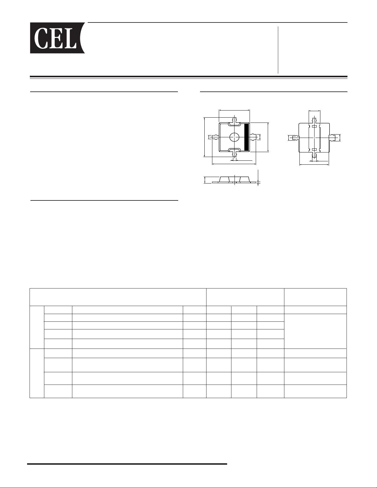
OUTLINE DIMENSIONS (Units in mm)
PACKAGE OUTLINE 79A
ELECTRICAL CHARACTERISTICS (TC = 25°C)
PART NUMBER NE6510179A
PACKAGE OUTLINE 79A
SYMBOLS CHARACTERISTICS UNITS MIN TYP MAX TEST CONDITIONS
POUT Output Power dBm 31.5 32.5
GL Linear Gain
1
dB 10.0
ηADD Power Added Efficiency % 50 58
ID Drain Current A 0.72
IDSS Saturated Drain Current A 2.4 VDS = 2.5 V; VGS = 0 V
VP Pinch-Off Voltage V -2.0 -0.4 VDS = 2.5 V; ID = 14 mA
RTH Thermal Resistance °C/W 5 8 Channel to Case
BVGD Gate to Drain Breakdown Voltage V 12 IGD = 14 mA
Functional
Characteristics
Electrical DC
Characteristics
Notes:
1. Pin = 0 dBm
2. DC performance is tested 100% . Several samples per wafer are tested for RF performance. Wafer rejection criteria for standard devices is 1
reject for several samples.
Note: Unless otherwise specified, tolerance is ±0.2 mm
f = 1900 MHz, VDS = 3.5 V,
Pin = +25 dBm, Rg = 100 Ω
IDSQ = 200 mA (RF OFF)
2
T
I
9
X
Source
Gate
Drain
4.2 MAX
5.7 MAX
4.4 MAX
0.8 – 0.15
0.6 – 0.15
5.7 MAX
0.4 – 0.15
Source
Gate
Drain
1.2
MAX
1.0 MAX
3.6 – 0.2
0.8 MAX
0.9 – 0.2
0.2 – 0.1
1.5 – 0.2
BOTTOM VIEW
California Eastern Laboratories
剩余10页未读,继续阅读


评论0
最新资源