没有合适的资源?快使用搜索试试~ 我知道了~
ds21q59技术资料
5星 · 超过95%的资源 需积分: 12 11 下载量 45 浏览量
2009-02-14
13:22:24
上传
评论
收藏 652KB PDF 举报
温馨提示
试读
76页
演示DS21q59 E1 SCT收发器的功能 包括DS21q59 SCT、变压器、Bantum、BNC和RJ48网络连接器以及终端无源元件 用于75Ω E1的BNC连接器 为120Ω E1提供Bantam和RJ48连接器 多抽头变压器,便于实现与75Ω及120Ω/100Ω通道的真正阻抗匹配 兼容于DK101或DK2000开发板母板 DK101/DK2000和ChipView软件提供点击访问DS21354寄存器设置 由软件控制(寄存器映射)配置开关,方便了时钟和信号路由 所有设备端成帧器引脚便于与外部数据源/接收器的连接 LED用于指示信号丢失、中断状态以及复用时钟和信号路由配置 易读的丝网印制标签可以辨别与所有连接器、跳针和LED相关的信号 网络接口具有过压和过流事件保护,可定制
资源推荐
资源详情
资源评论
1 of 76
REV: 090104
Note: Some revisions of this device may incorporate deviations from published specifications known as errata. Multiple revisions of any device
may be simultaneously available through various sales channels. For information about device errata, click here: www.maxim-ic.com/errata
.
GENERAL DESCRIPTION
The DS21Q59 E1 quad transceiver contains all the
necessary functions for connecting to four E1 lines.
The DS21Q59 is a direct replacement for the
DS21Q50, with the addition of signaling access and
improved interrupt handling. It is composed of a line
interface unit (LIU), framer, and a TDM backplane
interface, and is controlled through an 8-bit parallel
port configured for Intel or Motorola bus operations or
serial port operation.
APPLICATIONS
DSLAMs
Routers
IMA and WAN Equipment
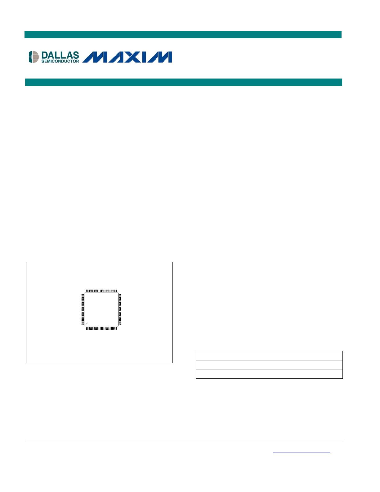
PIN CONFIGURATION
FEATURES
§ Four Complete E1 (CEPT) PCM-30/ISDN-PRI
Transceivers
§ Pin Compatible with the DS21Q50
§ Long-Haul and Short-Haul Line Interfaces
§ 32-Bit or 128-Bit Crystal-Less Jitter Attenuator
§ Frames to FAS, CAS, and CRC4 Formats
§ CAS/CCS Signaling Support
§ 4MHz/8MHz/16MHz Clock Synthesizer
§ Flexible System Clock with Automatic Source
Switching on Loss-of-Clock Source
§ Two-Frame Elastic-Store Slip Buffer on the
Receive Side
§ Interleaving PCM Bus Operation Up to
16.384MHz
§ Configurable Parallel and Serial Port Operation
§ Detects and Generates Remote and AIS Alarms
§ Fully Independent Transmit and Receive
Functionality
§ Four Separate Loopback Functions
§ PRBS Generation/Detection/Error Counting
§ 3.3V Low-Power CMOS
§ Large Counters for Bipolar and Code Violations,
CRC4 Codeword Errors, FAS Word Errors, and
E Bits
§ Eight Additional User-Configurable Output Pins
§ 100-Pin (14mm) LQFP Package
ORDERING INFORMATION
PART TEMP RANGE PIN-PACKAGE
DS21Q59L 0°C to +70°C 100 LQFP
DS21Q59LN -40°C to +85°C 100 LQFP
LQFP
1
100
Dallas
Semiconducto
r
DS21Q59
TOP VIEW
DS21Q59
E1 Quad Transceive
r
www.maxim-ic.com
DS21Q59 Quad E1 Transceiver
2 of 76
TABLE OF CONTENTS
1. ACRONYMS .......................................................................................................................6
2. DETAILED DESCRIPTION.................................................................................................6
3. BLOCK DIAGRAM .............................................................................................................7
4. PIN DESCRIPTION.............................................................................................................8
4.1 PIN FUNCTION DESCRIPTIONS......................................................................................................12
5. FUNCTIONAL DESCRIPTION .........................................................................................13
6. HOST INTERFACE PORT................................................................................................14
6.1 PARALLEL PORT OPERATION .......................................................................................................14
6.2 SERIAL PORT OPERATION ............................................................................................................14
7. REGISTER MAP...............................................................................................................16
8. CONTROL, ID, AND TEST REGISTERS .........................................................................17
8.1 POWER-UP SEQUENCE................................................................................................................18
8.2 FRAMER LOOPBACK ....................................................................................................................21
8.3 AUTOMATIC ALARM GENERATION .................................................................................................22
8.4 REMOTE LOOPBACK ....................................................................................................................22
8.5 LOCAL LOOPBACK .......................................................................................................................23
9. STATUS AND INFORMATION REGISTERS ...................................................................27
9.1 INTERRUPT HANDLING .................................................................................................................28
9.2 CRC4 SYNC COUNTER................................................................................................................29
10. ERROR COUNT REGISTERS..........................................................................................34
10.1 BPV OR CV COUNTER .............................................................................................................34
10.2 CRC4 ERROR COUNTER..........................................................................................................34
10.3 E-BIT/PRBS BIT-ERROR COUNTER ..........................................................................................35
10.4 FAS ERROR COUNTER.............................................................................................................35
11. SIGNALING OPERATION................................................................................................36
11.1 RECEIVE SIGNALING.................................................................................................................36
11.2 TRANSMIT SIGNALING...............................................................................................................36
11.3 CAS OPERATION .....................................................................................................................36
12. DS0 MONITORING FUNCTION .......................................................................................37
13. PRBS GENERATION AND DETECTION.........................................................................39
14. SYSTEM CLOCK INTERFACE ........................................................................................40
15. TRANSMIT CLOCK SOURCE..........................................................................................41
16. IDLE CODE INSERTION ..................................................................................................41
DS21Q59 Quad E1 Transceiver
3 of 76
17. PER-CHANNEL LOOPBACK ..........................................................................................42
18. ELASTIC STORE OPERATION .......................................................................................42
19. ADDITIONAL (Sa) AND INTERNATIONAL (Si) BIT OPERATION..................................43
20. USER-CONFIGURABLE OUTPUTS................................................................................45
21. LINE INTERFACE UNIT ...................................................................................................47
21.1 RECEIVE CLOCK AND DATA RECOVERY .....................................................................................47
21.1.1 Termination ...........................................................................................................................................47
21.2 TRANSMIT WAVESHAPING AND LINE DRIVING .............................................................................48
21.3 JITTER ATTENUATORS ..............................................................................................................50
21.3.1 Clock and Data Jitter Attenuators .........................................................................................................50
21.3.2 Undedicated Clock Jitter Attenuator .....................................................................................................51
22. CODE MARK INVERSION (CMI) .....................................................................................52
23. INTERLEAVED PCM BUS OPERATION .........................................................................54
24. FUNCTIONAL TIMING DIAGRAMS.................................................................................56
24.1 RECEIVE..................................................................................................................................56
24.2 TRANSMIT................................................................................................................................58
25. OPERATING PARAMETERS...........................................................................................62
26. AC TIMING PARAMETERS AND DIAGRAMS ................................................................63
26.1 MULTIPLEXED BUS AC CHARACTERISTICS.................................................................................63
26.2 NONMULTIPLEXED BUS AC CHARACTERISTICS ..........................................................................66
26.3 SERIAL PORT ...........................................................................................................................68
26.4 RECEIVE AC CHARACTERISTICS ...............................................................................................69
26.5 TRANSMIT AC CHARACTERISTICS .............................................................................................72
26.6 SPECIAL MODES AC CHARACTERISTICS ....................................................................................74
27. PACKAGE INFORMATION..............................................................................................75
28. REVISION HISTORY........................................................................................................76
DS21Q59 Quad E1 Transceiver
4 of 76
LIST OF FIGURES
Figure 3-1. Block Diagram....................................................................................................................... 7
Figure 6-1. Serial Port Operation Mode 1 ...............................................................................................14
Figure 6-2. Serial Port Operation Mode 2 ...............................................................................................15
Figure 6-3. Serial Port Operation Mode 3 ...............................................................................................15
Figure 6-4. Serial Port Operation Mode 4 ...............................................................................................15
Figure 21-1. External Analog Connections (Basic Configuration) ...........................................................48
Figure 21-2. External Analog Connections (Protected Interface) ............................................................49
Figure 21-3. Transmit Waveform Template ............................................................................................50
Figure 21-4. Jitter Tolerance...................................................................................................................51
Figure 21-5. Jitter Attenuation ................................................................................................................51
Figure 22-1. CMI Coding ........................................................................................................................52
Figure 22-2. Example of CMI Code Violation (CV)..................................................................................53
Figure 23-1. IBO Configuration Using Two DS21Q59 Transceivers (Eight E1 Lines)..............................55
Figure 24-1. Receive Frame and Multiframe Timing ...............................................................................56
Figure 24-2. Receive Boundary Timing (With Elastic Store Disabled).....................................................56
Figure 24-3. Receive Boundary Timing (With Elastic Store Enabled) .....................................................56
Figure 24-4. Receive Interleave Bus Operation ......................................................................................57
Figure 24-5. Transmit Frame and Multiframe Timing ..............................................................................58
Figure 24-6. Transmit Boundary Timing..................................................................................................58
Figure 24-7. Transmit Interleave Bus Operation .....................................................................................59
Figure 24-8. Framer Synchronization Flowchart .....................................................................................60
Figure 24-9. Transmit Data Flow ............................................................................................................61
Figure 26-1. Intel Bus Read AC Timing (PBTS = 0)................................................................................64
Figure 26-2. Intel Bus Write Timing (PBTS = 0)......................................................................................64
Figure 26-3. Motorola Bus AC Timing (PBTS = 1) ..................................................................................65
Figure 26-4. Intel Bus Read Timing (PBTS = 0)......................................................................................66
Figure 26-5. Intel Bus Write Timing (PBTS = 0)......................................................................................67
Figure 26-6. Motorola Bus Read Timing (PBTS = 1)...............................................................................67
Figure 26-7. Motorola Bus Write Timing (PBTS = 1)...............................................................................67
Figure 26-8. Serial Bus Timing (BTS1 = 1, BTS0 = 0) ............................................................................68
Figure 26-9. Receive AC Timing (Receive Elastic Store Disabled) .........................................................70
Figure 26-10. Receive AC Timing (Receive Elastic Store Enabled)........................................................71
Figure 22-11. Transmit AC Timing (IBO Disabled)..................................................................................73
Figure 22-12. Transmit AC Timing (IBO Enabled) ..................................................................................74
Figure 26-13. NRZ Input AC Timing .......................................................................................................74
DS21Q59 Quad E1 Transceiver
5 of 76
LIST OF TABLES
Table 4-A. Pin Description (Sorted by Function)...................................................................................... 8
Table 4-B. Pin Assignments (Sorted by Number) ...................................................................................10
Table 4-C. System (Backplane) Interface Pins .......................................................................................12
Table 4-D. Alternate Jitter Attenuator .....................................................................................................12
Table 4-E. Clock Synthesizer .................................................................................................................12
Table 4-F. Parallel Port Control Pins ......................................................................................................12
Table 4-G. Serial Port Control Pins.........................................................................................................13
Table 4-H. Line Interface Pins ................................................................................................................13
Table 4-I. Supply Pins ............................................................................................................................13
Table 6-A. Bus Mode Select ...................................................................................................................14
Table 7-A. Register Map (Sorted by Address) ........................................................................................16
Table 8-A. Sync/Resync Criteria.............................................................................................................19
Table 8-B. G.703 Function......................................................................................................................24
Table 8-C. Output Modes .......................................................................................................................25
Table 9-A. Alarm Criteria ........................................................................................................................29
Table 13-A. Transmit PRBS Mode Select...............................................................................................39
Table 13-B. Receive PRBS Mode Select................................................................................................39
Table 14-A. Synthesizer Output Select...................................................................................................40
Table 14-B. System Clock Selection.......................................................................................................40
Table 20-A. OUTA and OUTB Function Select.......................................................................................46
Table 21-A. Line Build-Out Select in LICR..............................................................................................48
Table 21-B. Transformer Specifications..................................................................................................48
Table 23-A. IBO System Clock Select ....................................................................................................54
Table 23-B. IBO Device Assignment ......................................................................................................54
Table 26-A. AC Characteristics—Multiplexed Parallel Port.....................................................................63
Table 26-B. AC Characteristics—Nonmultiplexed Parallel Port ..............................................................66
Table 26-C. AC Characteristics—Serial Port (BTS1 = 1, BTS0 = 0) .......................................................68
Table 26-D. AC Characteristics—Receiver.............................................................................................69
Table 26-E. AC Characteristics—Transmit .............................................................................................72
Table 26-F. AC Characteristics—Special Modes ....................................................................................74
剩余75页未读,继续阅读
资源评论
- lifesky20062023-02-06学习资料,借鉴参考
- knowmuch2013-01-21该资源就是官网上的器件手册。
- ima_zhan2013-09-13不错,有用处
renlei1029
- 粉丝: 3
- 资源: 4
上传资源 快速赚钱
- 我的内容管理 展开
- 我的资源 快来上传第一个资源
- 我的收益 登录查看自己的收益
- 我的积分 登录查看自己的积分
- 我的C币 登录后查看C币余额
- 我的收藏
- 我的下载
- 下载帮助
最新资源
- 基于matlab实现对表面肌电信号进行归一化处理,并对归一化后的图形显示 .rar
- 基于matlab实现单级倒立摆的 T-S 模型 包括 LMI 程序源码
- 图书管理系统(struts+hibernate+spring+ext).rar
- 基于matlab实现此压缩包包含语音信号处理中的语音变声代码加音频.rar
- STM32使用PWM驱动舵机并通过OLED显示
- 基于matlab实现车辆路径规划;遗传算法;matlab代码.rar
- 图书管理系统(struts+hibernate+spring)130225.rar
- 基于matlab实现采用标量衍射理论,实现菲涅尔衍射和夫琅禾费衍射,对光波的波前传播和数字全息的应用有帮助.rar
- JavaScript版去除链表重复元素
- 微信小程序项目-功德木鱼(带设置面板-自定义文字、可选字体颜色、可选木鱼样式)
资源上传下载、课程学习等过程中有任何疑问或建议,欢迎提出宝贵意见哦~我们会及时处理!
点击此处反馈
安全验证
文档复制为VIP权益,开通VIP直接复制
信息提交成功