2003 Jun 30 2
Philips Semiconductors Product specification
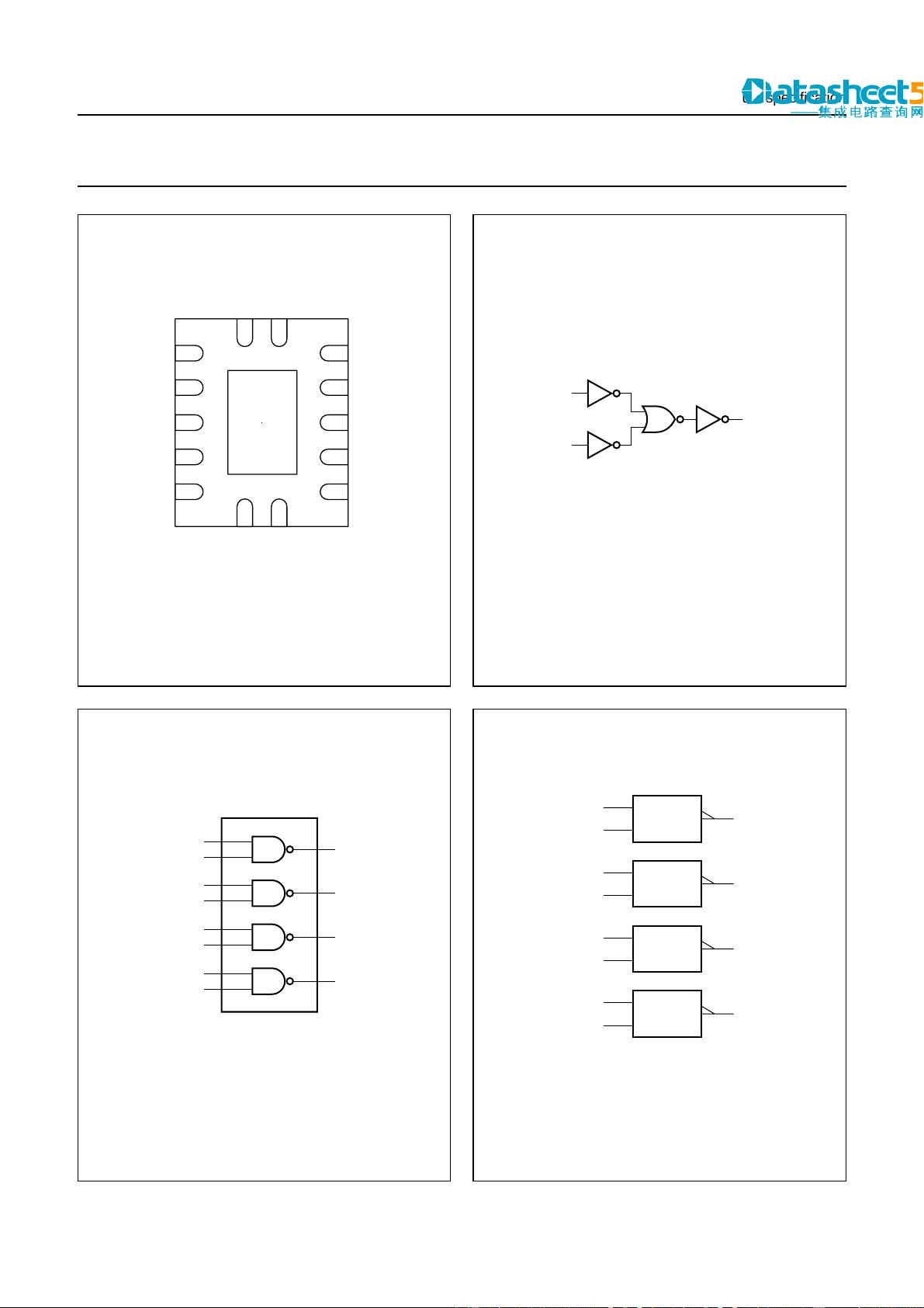
Quad 2-input NAND gate 74HC00; 74HCT00
FEATURES
• Complies with JEDEC standard no. 8-1A
• ESD protection:
HBM EIA/JESD22-A114-A exceeds 2000 V
MM EIA/JESD22-A115-A exceeds 200 V
• Specified from −40 to +85 °C and −40 to +125 °C.
DESCRIPTION
The 74HC00/74HCT00 are high-speed Si-gate CMOS
devices and are pin compatible with low power Schottky
TTL (LSTTL). They are specified in compliance with
JEDEC standard no. 7A.
The 74HC00/74HCT00 provide the 2-input NAND
function.
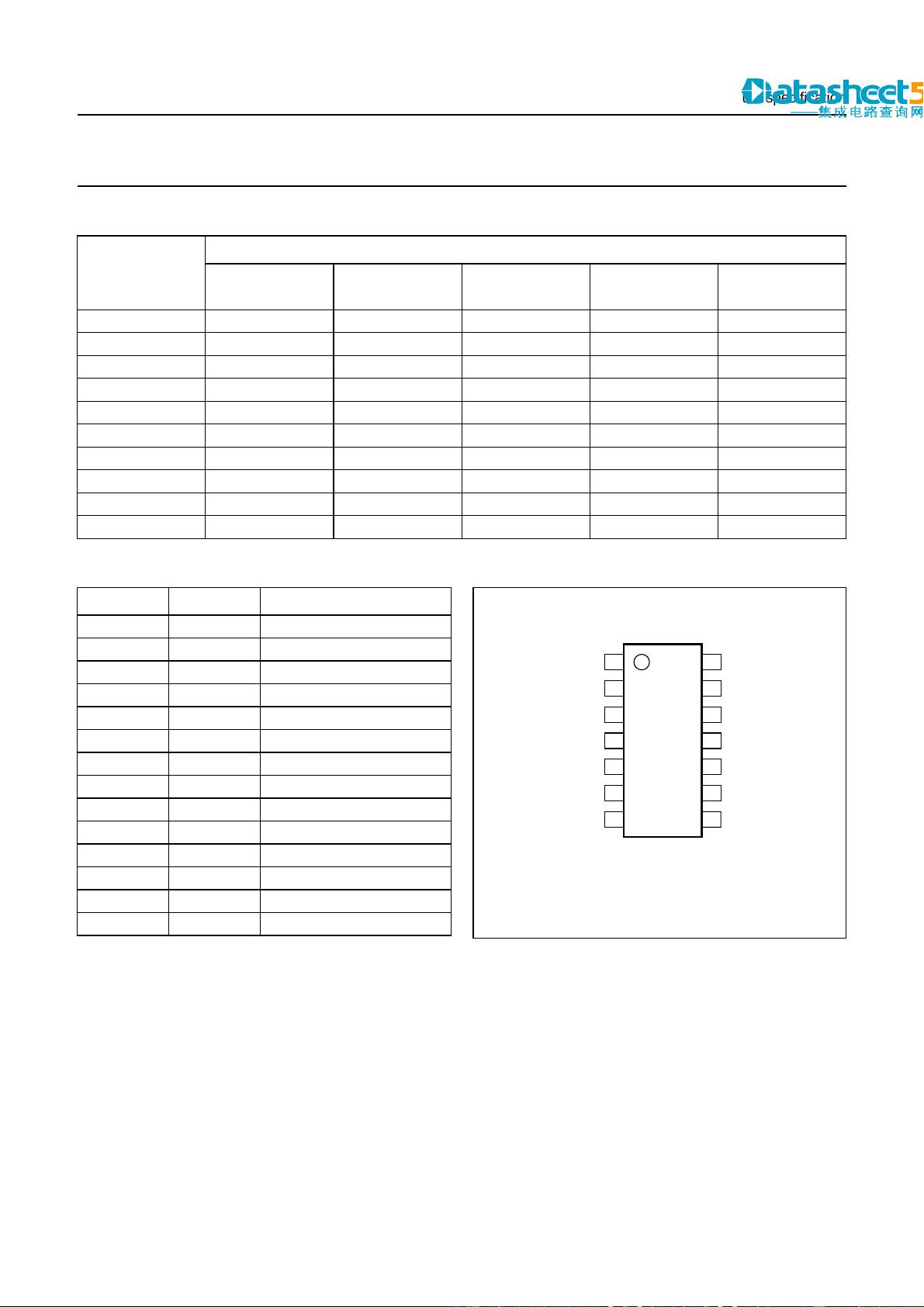
QUICK REFERENCE DATA
GND = 0 V; T
amb
=25°C; t
r
=t
f
= 6 ns.
Notes
1. C
PD
is used to determine the dynamic power dissipation (P
D
in µW).
P
D
=C
PD
× V
CC
2
× f
i
× N+Σ(C
L
× V
CC
2
× f
o
) where:
f
i
= input frequency in MHz;
f
o
= output frequency in MHz;
C
L
= output load capacitance in pF;
V
CC
= supply voltage in Volts;
N = total load switching outputs;
Σ(C
L
× V
CC
2
× f
o
) = sum of the outputs.
2. For 74HC00 the condition is V
I
= GND to V
CC
.
For 74HCT00 the condition is V
I
= GND to V
CC
− 1.5 V.
FUNCTION TABLE
See note 1.
Note
1. H = HIGH voltage level;
L = LOW voltage level.
SYMBOL PARAMETER CONDITIONS
TYPICAL
UNIT
74HC00 74HCT00
t
PHL
/t
PLH
propagation delay nA, nB to nY C
L
= 15 pF; V
CC
= 5 V 7 10 ns
C
I
input capacitance 3.5 3.5 pF
C
PD
power dissipation capacitance per gate notes 1 and 2 22 22 pF
INPUT OUTPUT
nA nB nY
LLH
LHH
HLH
HHL