没有合适的资源?快使用搜索试试~ 我知道了~
IR2125-芯片资料介绍.pdf
1.该资源内容由用户上传,如若侵权请联系客服进行举报
2.虚拟产品一经售出概不退款(资源遇到问题,请及时私信上传者)
版权申诉
0 下载量 138 浏览量
2022-07-04
09:53:27
上传
评论
收藏 185KB PDF 举报
温馨提示
试读
16页
IR2125-芯片资料介绍.pdf
资源推荐
资源详情
资源评论
Features
• Floating channel designed for bootstrap operation
Fully operational to +500V
Tolerant to negative transient voltage
dV/dt immune
• Gate drive supply range from 12 to 18V
• Undervoltage lockout
• Current detection and limiting loop to limit driven
power transistor current
• Error lead indicates fault conditions and programs
shutdown time
• Output in phase with input
• 2.5V, 5V and 15V input logic compatible
Description
The IR2125(S) is a high voltage, high speed power
MOSFET and IGBT driver with over-current limiting
protection circuitry. Proprietary HVIC and latch im-
mune CMOS technologies enable ruggedized mono-
lithic construction. Logic inputs are compatible with
standard CMOS or LSTTL outputs, down to 2.5V
logic. The output driver features a high pulse current
buffer stage designed for minimum driver cross-
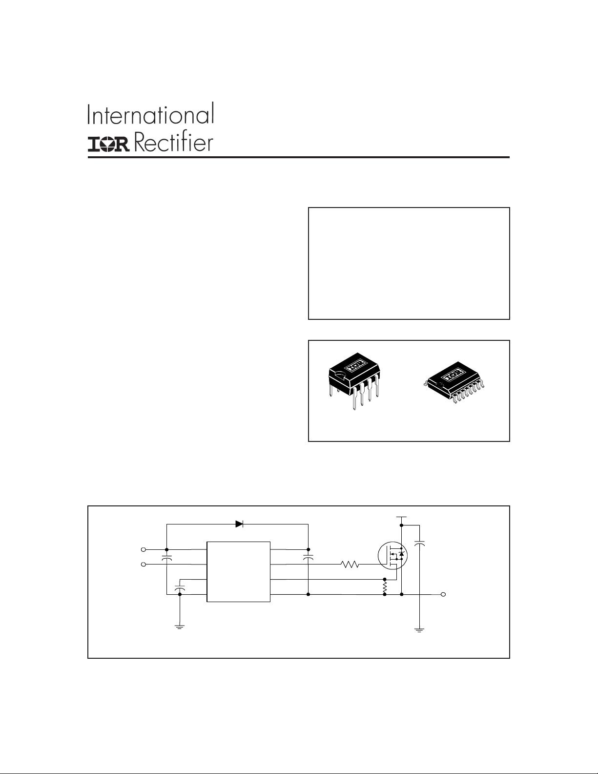
CURRENT LIMITING SINGLE CHANNEL DRIVER
Product Summary
V
OFFSET
500V max.
I
O
+/- 1A / 2A
V
OUT
12 - 18V
V
CSth
230 mV
t
on/off
(typ.) 150 & 150 ns
Packages
Typical Connection
conduction. The protection circuitry detects over-current in the driven power transistor and limits the gate drive volt-
age. Cycle by cycle shutdown is programmed by an external capacitor which directly controls the time interval
between detection of the over-current limiting conditions and latched shutdown. The floating channel can be used to
drive an N-channel power MOSFET or IGBT in the high or low side configuration which operates up to 500 volts.
V
CC
V
B
CS
OUT
V
S
COM
IN
ERR
V
CC
IN
TO
LOAD
up to 500V
IR2125
(
S
)
Data Sheet No. PD60017-M
www.irf.com 1
(Refer to Lead Assignments for correct pin configuration). This/These diagram(s) show electrical
connections only. Please refer to our Application Notes and DesignTips for proper circuit board layout.
8-Lead PDIP
16-Lead SOIC
(Wide Body)
IR2125
(
S
)
2 www.irf.com
Symbol Definition Min. Max. Units
V
B
High Side Floating Supply Voltage -0.3 525
V
S
High Side Floating Offset Voltage V
B
- 25 V
B
+ 0.3
V
HO
High Side Floating Output Voltage V
S
- 0.3 V
B
+ 0.3
V
CC
Logic Supply Voltage -0.3 25 V
V
IN
Logic Input Voltage -0.3 V
CC
+ 0.3
V
ERR
Error Signal Voltage -0.3 V
CC
+ 0.3
V
CS
Current Sense Voltage V
S
- 0.3 V
B
+ 0.3
dV
s
/dt Allowable Offset Supply Voltage Transient — 50 V/ns
P
D
Package Power Dissipation @ T
A
≤ +25°C (8 lead PDIP) — 1.0
(16 lead SOIC) — 1.25
Rth
JA
Thermal Resistance, Junction to Ambient (8 lead PDIP) — 125
(16lLead SOIC) — 100
T
J
Junction Temperature — 150
T
S
Storage Temperature -55 150
T
L
Lead Temperature (Soldering, 10 seconds) — 300
Absolute Maximum Ratings
Absolute Maximum Ratings indicate sustained limits beyond which damage to the device may occur. All voltage param-
eters are absolute voltages referenced to COM. The Thermal Resistance and Power Dissipation ratings are measured
under board mounted and still air conditions.
Symbol Definition Min. Max. Units
V
B
High Side Floating Supply Voltage V
S
+ 12 V
S
+ 18
V
S
High Side Floating Offset Voltage Note 1 500
V
HO
High Side Floating Output Voltage V
S
V
B
V
CC
Logic Supply Voltage 0 18
V
IN
Logic Input Voltage 0 V
CC
V
ERR
Error Signal Voltage 0 V
CC
V
CS
Current Sense Signal Voltage V
S
V
B
T
A
Ambient Temperature -40 125 °C
Note 1: Logic operational for V
S
of -5 to +500V. Logic state held for V
S
of -5V to -V
BS
. (Please refer to the Design Tip
DT97-3 for more details).
Recommended Operating Conditions
The Input/Output logic timing diagram is shown in Figure 1. For proper operation the device should be used within the
recommended conditions. The V
S
offset rating is tested with all supplies biased at 15V differential.
W
°C/W
°C
V
www.irf.com 3
IR2125
(
S
)
Symbol Definition Figure Min. Typ. Max. Units Test Conditions
V
IH
Logic “1” Input Voltage 14 2.2 — —
V
IL
Logic “0” Input Voltage 15 — — 0.8
V
CSTH+
CS Input Positive Going Threshold 16 150 230 320
V
CSTH-
CS Input Negative Going Threshold 17 130 200 260
V
OH
High Level Output Voltage, V
BIAS
- V
O
18 — — 100 I
O
= 0A
V
OL
Low Level Output Voltage, V
O
19 — — 100 I
O
= 0A
I
LK
Offset Supply Leakage Current 20 — — 50 V
B
= V
S
= 500V
I
QBS
Quiescent V
BS
Supply Current 21 — 400 1000 V
IN
= V
CS
= 0V or 5V
I
QCC
Quiescent V
CC
Supply Current 22 — 700 1200 V
IN
= V
CS
= 0V or 5V
I
IN+
Logic “1” Input Bias Current 23 — 4.5 10 µA V
IN
= 5V
I
IN-
Logic “0” Input Bias Current 24 — — 1.0 V
IN
= 0V
I
CS+
“High” CS Bias Current 25 — 4.5 10 V
CS
= 3V
I
CS-
“Low” CS Bias Current 26 — — 1.0 V
CS
= 0V
V
BSUV+
V
BS
Supply Undervoltage Positive Going 27 8.5 9.2 10.0
Threshold
V
BSUV-
V
BS
Supply Undervoltage Negative Going 28 7.7 8.3 9.0
Threshold
V
CCUV+
V
CC
Supply Undervoltage Positive Going 29 8.3 8.9 9.6
Threshold
V
CCUV-
V
CC
Supply Undervoltage Negative Going 30 7.3 8.0 8.7
Threshold
I
ERR
ERR Timing Charge Current 31 65 100 130 V
IN
= 5V, V
CS
= 3V
ERR < V
ERR+
I
ERR+
ERR Pull-Up Current 32 8.0 15 — V
IN
= 5V, V
CS
= 3V
ERR > V
ERR+
I
ERR-
ERR Pull-Down Current 33 16 30 — V
IN
= 0V
I
O+
Output High Short Circuit Pulsed Current 34 1.0 1.6 — V
O
= 0V, V
IN
= 5V
PW ≤ 10 µs
I
O-
Output Low Short Circuit Pulsed Current 35 2.0 3.3 — V
O
= 15V, V
IN
= 0V
PW ≤ 10 µs
V
mV
mA
V
µA
A
Static Electrical Characteristics
V
BIAS
(V
CC
, V
BS
) = 15V and T
A
= 25°C unless otherwise specified. The V
IN
, V
TH
and I
IN
parameters are referenced to
COM. The V
O
and I
O
parameters are referenced to V
S
.
Dynamic Electrical Characteristics
V
BIAS
(V
CC
, V
BS
) = 15V, C
L
= 3300 pF and T
A
= 25°C unless otherwise specified. The dynamic electrical characteristics
are measured using the test circuit shown in Figures 3 through 6.
Symbol Definition Figure Min. Typ. Max. Units Test Conditions
t
on
Turn-On Propagation Delay 7 — 150 200 V
IN
= 0 & 5V
V
S
= 0 to 600V
t
off
Turn-Off Propagation Delay 8 — 150 190
t
sd
ERR Shutdown Propagation Delay 9 — 1.7 2.2 µs
t
r
Turn-On Rise Time 10 — 43 60
t
f
Turn-Off Fall Time 11 — 26 35
t
cs
CS Shutdown Propagation Delay 12 — 0.7 1.2
t
err
CS to ERR Pull-Up Propagation Delay 13 — 9.0 12 C
ERR
= 270 pF
ns
µs
ns
剩余15页未读,继续阅读
资源评论
书博教育
- 粉丝: 1
- 资源: 2836
上传资源 快速赚钱
- 我的内容管理 展开
- 我的资源 快来上传第一个资源
- 我的收益 登录查看自己的收益
- 我的积分 登录查看自己的积分
- 我的C币 登录后查看C币余额
- 我的收藏
- 我的下载
- 下载帮助
最新资源
- Android基础面试题(附赠答案赠送版).md
- Vci.db
- 世界各国-经济距离数据汇总(2005-2022年).xlsx
- 基于Pytorch实现Kaggle竞赛“猫狗分类”源码+数据集(准确率超过99%).zip
- 基于SpringBoot实现的协同过滤美食推荐系统【源码+运行视频+论文】.rar
- 基于SpringBoot+Vue前后端分离型图书管理系统源码+数据库脚本(95分以上).zip
- com.wakdev.nfctasks.apk
- java毕业设计基于SpringBoot+Vue前后端分离型图书管理系统源码+数据库脚本.zip
- 机械与电气信息学院+电子信息工程本2002班+王梦亚+刘现伟+初稿(2).doc
- 中国各地级市的海拔标准差数据集.xlsx
资源上传下载、课程学习等过程中有任何疑问或建议,欢迎提出宝贵意见哦~我们会及时处理!
点击此处反馈
安全验证
文档复制为VIP权益,开通VIP直接复制
信息提交成功