lm393A-芯片资料介绍.PDF
版权申诉
76 浏览量
2022-07-04
09:08:22
上传
评论
收藏 323KB PDF 举报

LM193/LM293/LM393/LM2903
Low Power Low Offset Voltage Dual Comparators
General Description
The LM193 series consists of two independent precision
voltage comparators with an offset voltage specification as
low as 2.0 mV max for two comparators which were de-
signed specifically to operate from a single power supply
over a wide range of voltages. Operation from split power
supplies is also possible and the low power supply current
drain is independent of the magnitude of the power supply
voltage. These comparators also have a unique characteris-
tic in that the input common-mode voltage range includes
ground, even though operated from a single power supply
voltage.
Application areas include limit comparators, simple analog to
digital converters; pulse, squarewave and time delay gen-
erators; wide range VCO; MOS clock timers; multivibrators
and high voltage digital logic gates. The LM193 series was
designed to directly interface with TTL and CMOS. When op-
erated from both plus and minus power supplies, the LM193
series will directly interface with MOS logic where their low
power drain is a distinct advantage over standard compara-
tors.
Advantages
n High precision comparators
n Reduced V
OS
drift over temperature
n Eliminates need for dual supplies
n Allows sensing near ground
n Compatible with all forms of logic
n Power drain suitable for battery operation
Features
n Wide supply
— Voltage range: 2.0V to 36V
— single or dual supplies:
±
1.0V to
±
18V
n Very low supply current drain (0.4 mA) — independent
of supply voltage
n Low input biasing current: 25 nA
n Low input offset current:
±
5nA
n Maximum offset voltage:
±
3mV
n Input common-mode voltage range includes ground
n Differential input voltage range equal to the power
supply voltage
n Low output saturation voltage,: 250 mV at 4 mA
n Output voltage compatible with TTL, DTL, ECL, MOS
and CMOS logic systems
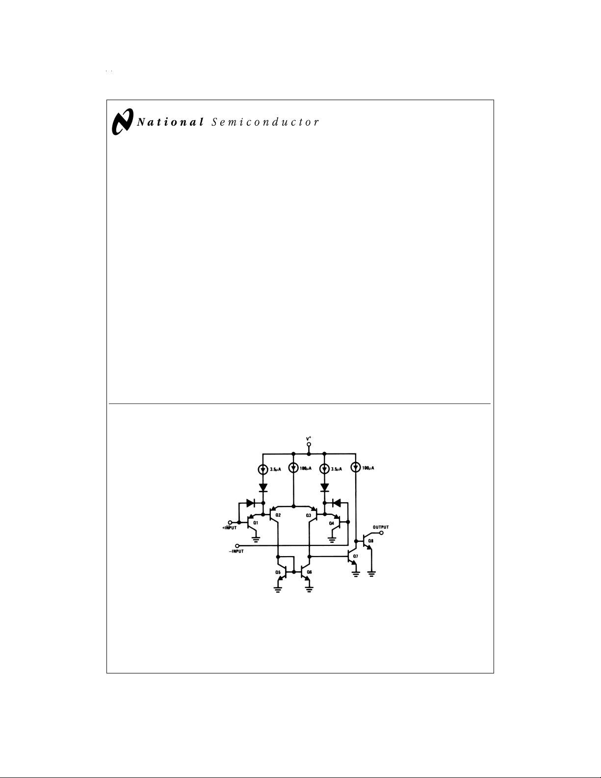
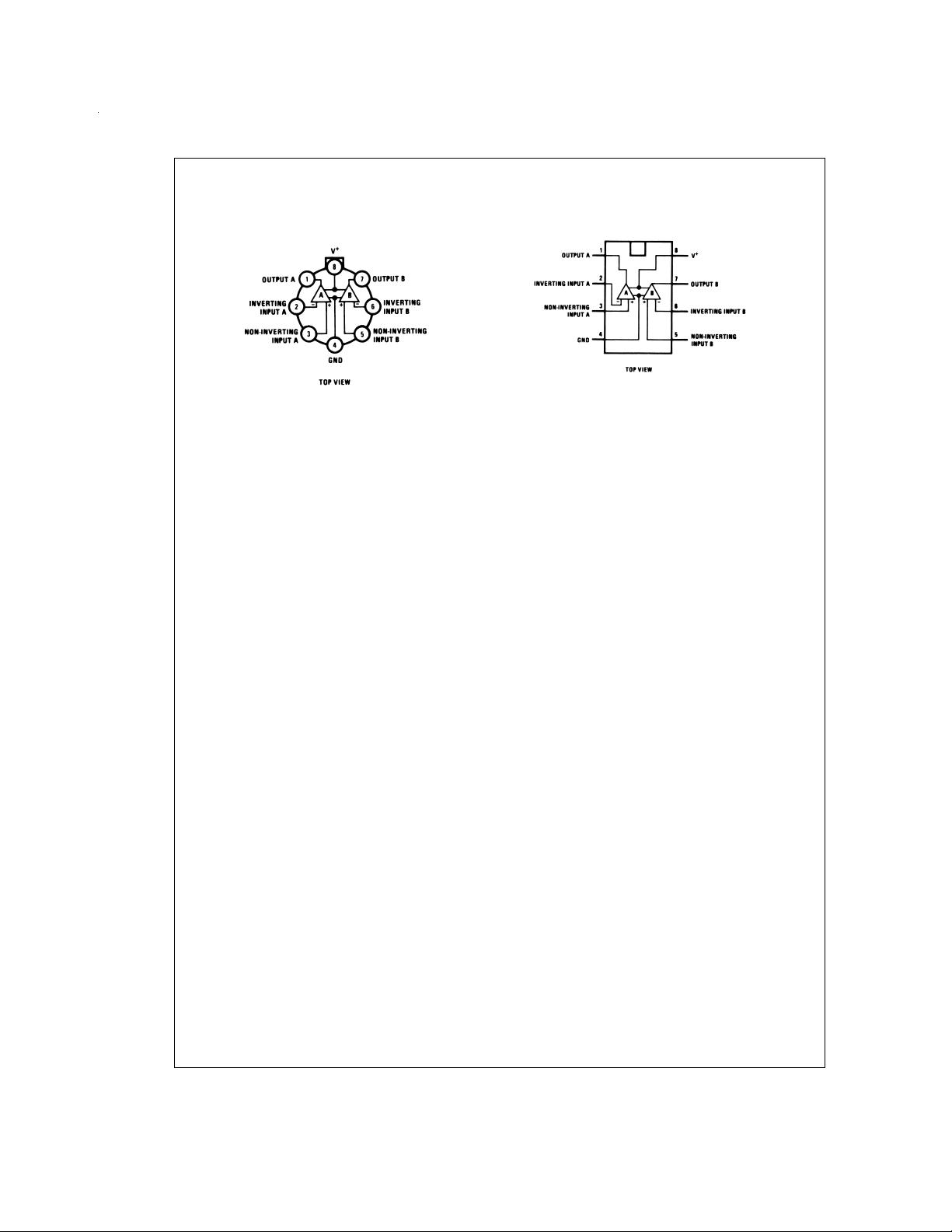
Schematic and Connection Diagrams
DS005709-2
May 1999
LM193/LM293/LM393/LM2903 Low Power Low Offset Voltage Dual Comparators
© 1999 National Semiconductor Corporation DS005709 www.national.com
剩余13页未读,继续阅读
资源评论


书博教育
- 粉丝: 1
- 资源: 2837


